Introduction
With Labs 01 through 04, you should have ended up with a complete schematic for your FM radio project - congrats! Now that your entire circuit is in Altium’s schematic editor, we can assign it to a PCB document and begin the board layout process.
Transferring Schematic to Layout
Running Schematic ERC
First things first - we want to make sure that our schematic looks good and makes electrical sense before we conduct the schematic-layout transfer. We can do this by running an Electrical Rules Check (ERC). It’ll follow a bunch of default rules that Altium has setup that check for issues in our schematic such as:
- Unconnected pins,
- Connections between mismatched pin types (e.g., an output pin connected to an output pin),
- Cosmetic problems with the schematic sheet, and
- Missing symbol details.
After finding issues via the ERC check, we can view and address them one-by-one to ensure our schematic is in tip-top shape.
To run ERC, right-click on your FMRadio_[your kerb].PrjPcb project in the Projects panel and run Validate PCB Project FMRadio_[your kerb].PrjPCB.
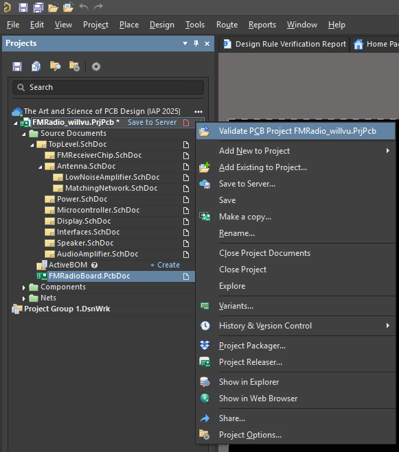
Afterwards, warnings and errors from the ERC will appear in the Messages panel. Errors must be resolved in order to continue into layout, but warnings can technically be left unaddressed and won’t stop the schematic-layout transfer process. However, for this lab you want to resolve both. Double-clicking on an error/warning will allow you to zoom into the location where it is occurring. In the example below, it shows where there is an unconnected GND power symbol.
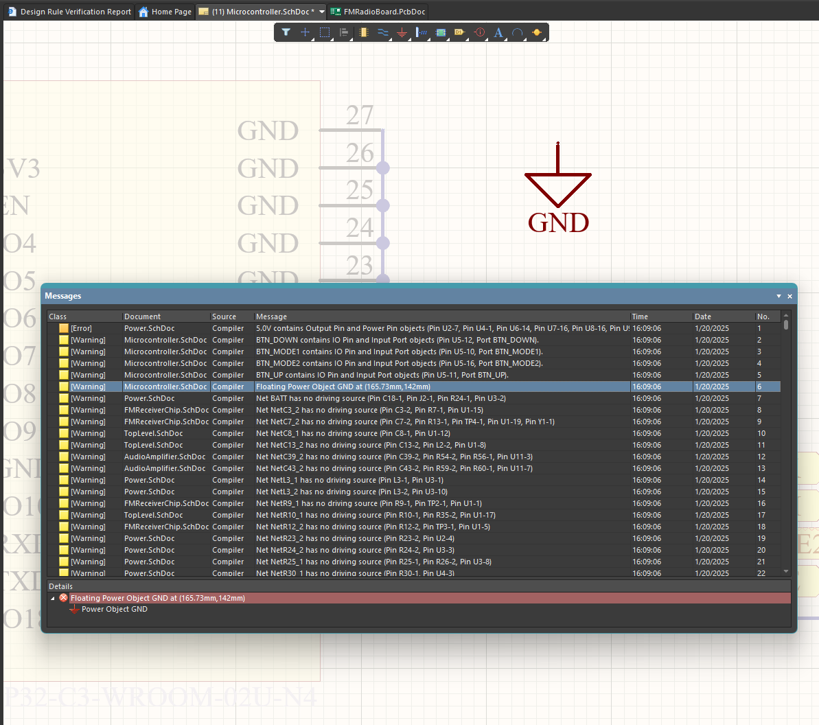
Fixing the issue and running ERC again will cause the error/warning to disappear. Use this to your advantage and resolve any errors or warnings in your schematic.
- Net has no driving source (typically is caused by an input/output pin being attached to a passive pin)
- Off grid net label or pin (the net label or pin is not neatly placed on the schematic sheet grid)
- Net has multiple names (given that the stated differing net names are of two differently named ports/sheet entires that should be connected to each other).
- Net contains IO pin and Input Port objects (only if the nets and pins are referring to the
Interfacesbuttons).
Forward Annotation
Forward annotation refers to using our schematic to update the what should be on our layout (there is also backwards annotation for updating the schematic from the layout, but this is a less common practice). With the schematic fully validated, we can conduct a forward annotation.
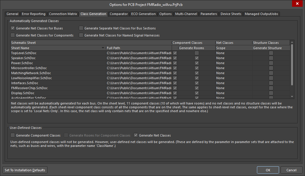
First, we need to configure Altium to add rooms in our forward annotation. Rooms are rectangular boxes in our layout that represent a sheet from our schematic (e.g., Power or AudioAmplifier). They hold all of the components within their respective sheet and are very useful for organizing our layout into distinct, functional areas.
To have Altium generate rooms during forward annotation, select Project->Project Options->Class Generation and select the checkbox for Generate Rooms for every sheet except the TopLevel sheet.
With the rooms option setup, we can continue the process of forward annotation by adding a PCB Document to the project.
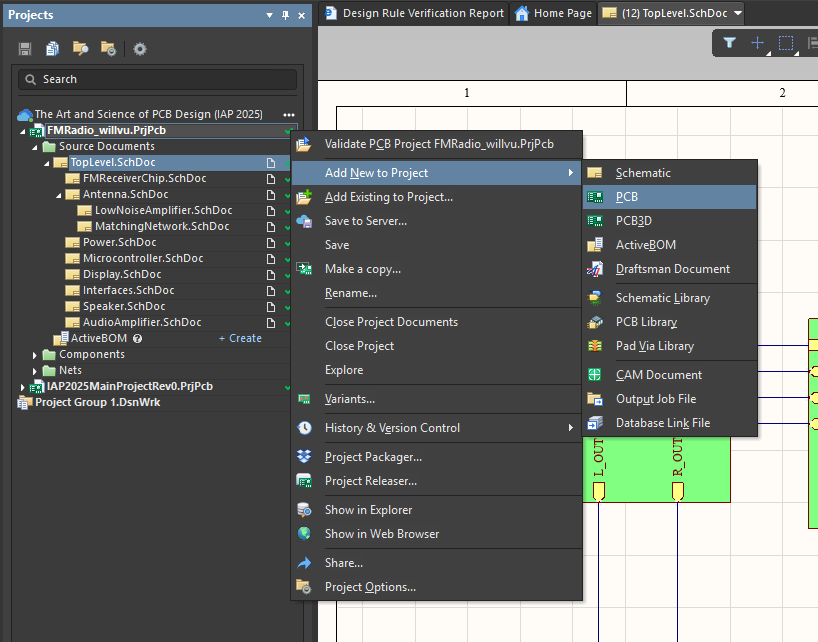
Name the PCB document FMRadioBoard.PcbDoc and return to any schematic sheet.
Afterwards, conduct a forward annotation by running Design->Update PCB Document FMRadioBoard.PcbDoc. This will produce an Engineering Change Order with all of the changes that will be copied from the schematic to the layout. Execute the changes.
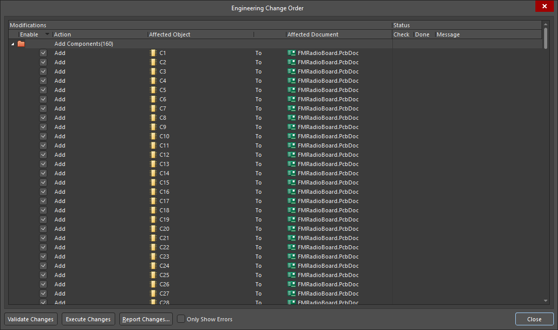
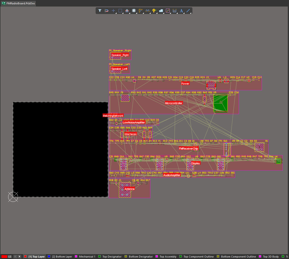
You should end up with the generic Altium board outline (a black rectangle, note that it may not be the same size and location as the one shown below) and all of board’s component’s footprints within their respective sheets/rooms placed onto the PCB document.
Preparing the Board
After having placed all of the schematic components onto the board via forward annotation, we can begin layout - woohoo!
Setting the Stackup
If you recall from Lecture 05, our first step in a PCB layout is configuring the board stackup. It’s mainly crucial to setting the number of copper layers we can use for routing, but it can also help us determine stackup-related factors such as impedance-controlled traces.
To access it, hit Design->Layer Stack Manager.... The Altium default is pretty close to what we want, but we still will want to make some adjustments. Add an ENIG (Nickel, Gold) surface finish layer above/below the two copper layers.
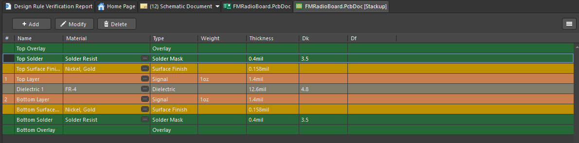
Afterwards, adjust the stackup so that it follows the two-layer stackup used by OSHPark1. Ignore the silkscreen part of the stackup as that cannot be adjusted in the Layer Stack Manager.
Additionally, use the FR4 substrate’s datasheet, linked on the same OSHPark two-layer stackup page, to determine the subtrate’s dielectric constant2 at 1 GHz and input it accordingly into the Layer Stack Manager.
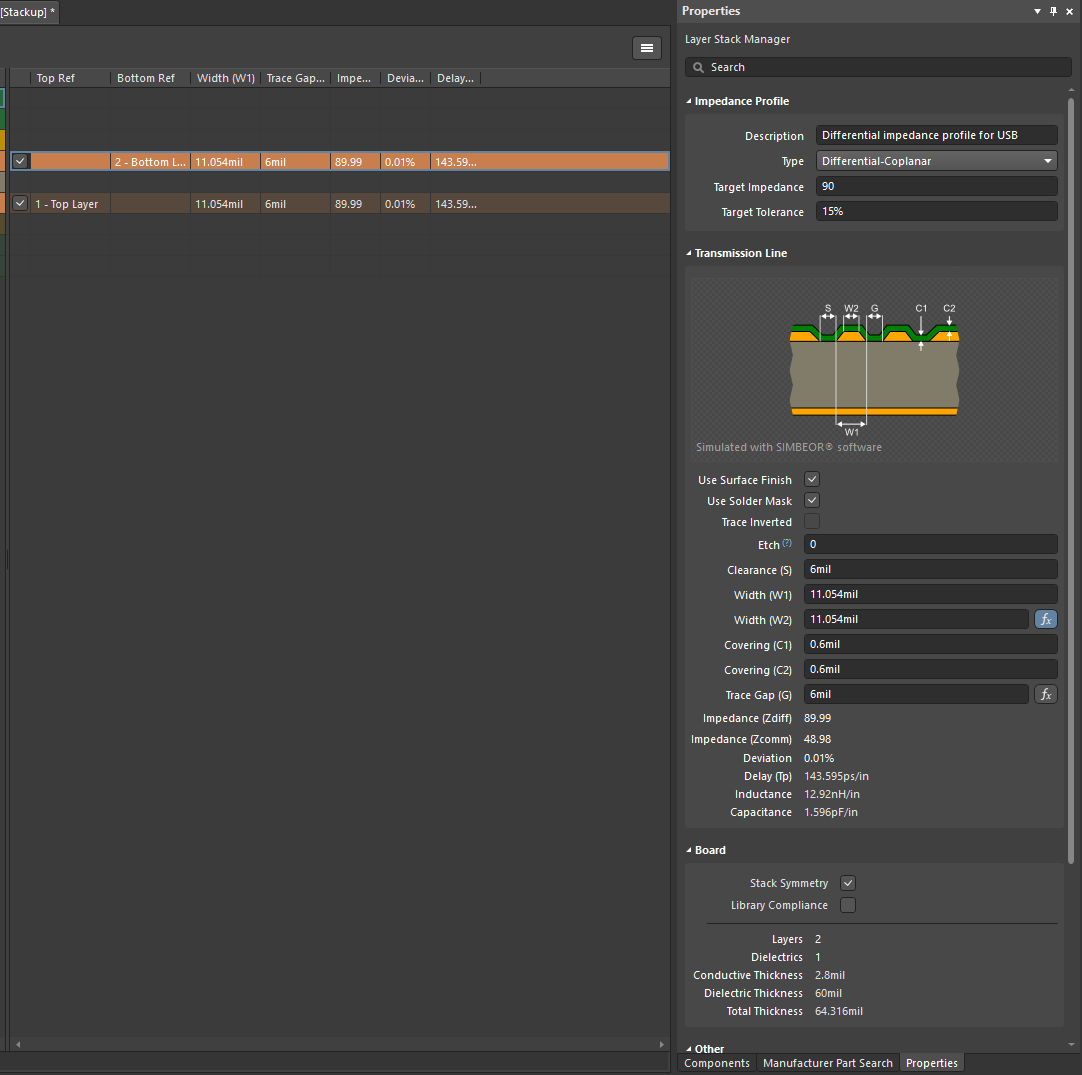
With the stackup set, we can use it to create an impedance profile that can be used to properly route differential pairs (used by the USB connection) later.
Within the Layer Stack Manager, click on the Impedance tab located at the bottom of the window. Add an impedance profile for the top layer that matches what is shown below. Note that the widths (W1 and W2) should be automatically calculated for you as you input the other parameters, so you should not input the width parameters yourself. If the calculated width values do not match what is shown below, it means your stackup is incorrect.
Adjusting the Board Shape
Next is our configuring the physical shape of our board. We can make the shape of the board anything we want, but let’s keep it simple and give ourselves plenty of room by having it be a 100 mm by 100 mm square (which is the maximum board size for many low-cost manufacturers before additional costs are added).
You can configure the board’s shape by drawing a shape primitive then assigning it to be the board outline.
Begin by drawing a 100 mm by 100 mm rectangle on the Mechanical 1 layer with the bottom left corner at the origin (the circle with the crosshair). It should match what is show below:
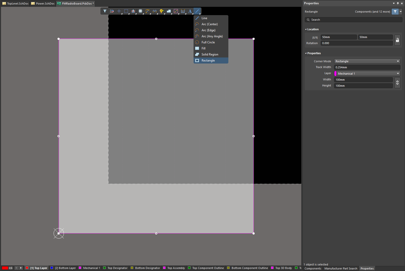
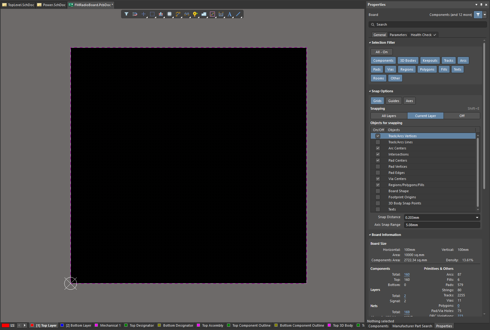
Subsequently, select the rectangle and click Design->Board Shape->Define Board Shape From Selected Objects. This should leave you with a new board shape and the Board Information section of the PCB document’s properties should reflect the new board size
Mounting Holes
Along with the board shape, we should also take the time to define other mechanical features, such as mounting holes.
Use 4 pads with 3.5 mm holes size to create 4 mounting holes (with their centers offset 4 mm from the edge) as shown below. Be sure to attach them to the GND net.
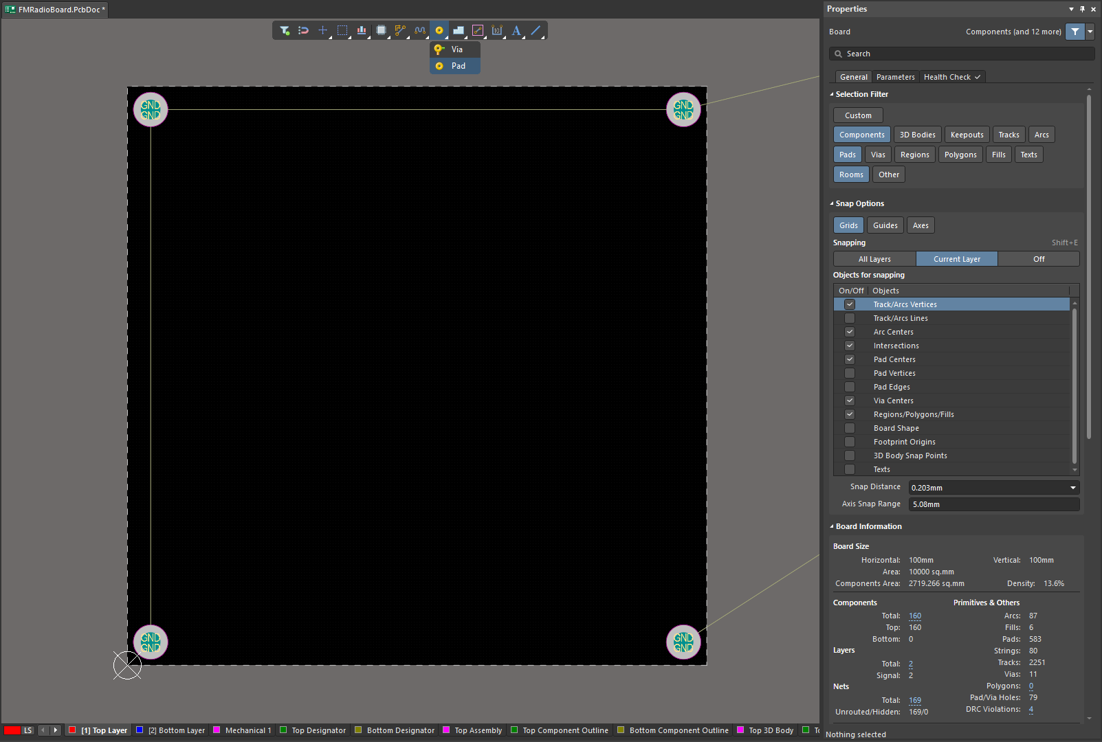
With these mounting holes, we should be able to use M3 screws to mount the board somewhere using standoffs if we need to.
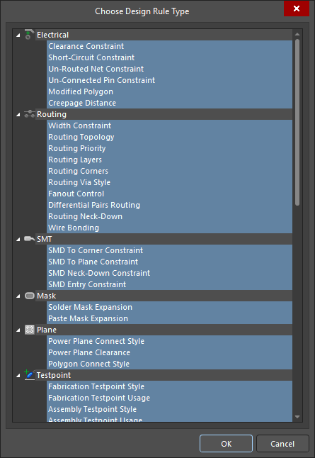
Configuring DRC Rules
The final step before components can actually be connected together on the board is to define the rules that will be used in the design rules check (DRC). Such rules help ensure that the board will work electrically and is manufacturable. The rules typically include details such as:
- Clearance
- Via size
- Trace width
- Copper pour style
Since Altium helps us adhere to DRC rules as we conduct our layout (such as by automatically selecting a legal trace width that aligns with DRC rules during routing), we want to set up the rules prior to any board work. Once again, we’ll use OSHPark’s two-layer board specifications to define our DRC rules.
Luckily for us, OSHPark provides a .RUL file for their two-layer stackups specifically for Altium Designer. Download the .RUL file. To import the rules, select Design->Rules... then right-click the Design Rules folder and select Import Rules....
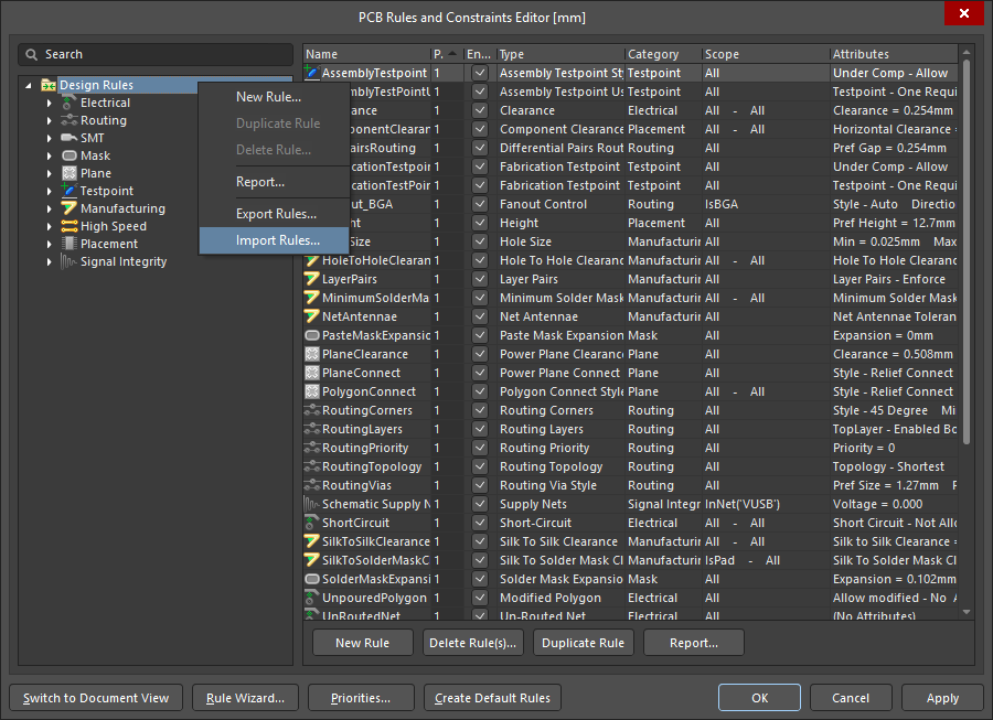
This will lead you to a dialog with every rule. Select all of the rules via CTRL-A,hit OK and select the .RUL file. Afterwards, have the rule import clear all existing rules and you’re done!
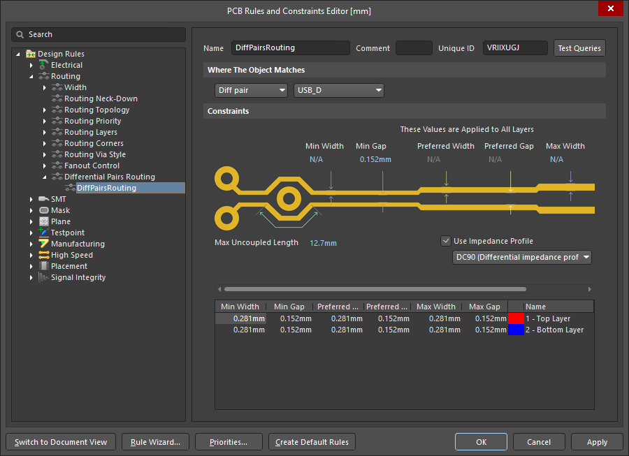
With the OSHPark rules imported, there is just one rule that we have to adjust manually: the differential pair routing rule for the USB lines. We want the rule to reflect the clearance and width constraints that we created for the USB differential pair when we created an impedance profile for it.
Go back into Design->Rules... and adjust the DiffPairsRouting rule to match what is show below:
Organizing Board Components
Looking at what has been completed so far with our board:
- Schematic Forward Annotation? ✅
- Stackup? ✅
- Board Shape? ✅
- Mounting Holes? ✅
- DRC Rules? ✅
Now we can get into putting the layout together!
At this point, you have some more flexibility as to how you decide you would like to layout the board, but the following instructions will suggest a setup that maximizes performance and ease-of-routing. No matter how you decide you’d like to approach the board’s routing, it’s first a good practice to utilize the hierarchical block diagram abstraction we created in our schematic to guide the way we do the layout.
We’ll first begin this by organizing the structure of our board, determining what parts of the FM radio should go where, before we try to connect nets or components together. Once we have arranged our board to have components where we want them to be, we’ll then start routing traces and creating connections.
Partitioning the Board
Thinking back to Lecture 05 and 06, we had some key takeaways. Mainly that:
- We should section off different board functions into their own areas (following the top-level block diagram structure of our schematic closely),
- Keep noisy components or sections (e.g., power supplies, actuators) physically distant from sensitive ones (e.g., analog devices, high-speed digital ICs) within the board, and
- Keep circuits compact and connections short throughout the board.
To this end, we can arrange our rooms as shown below. This setup should maximize the distance between the sensitive FM radio receiver chip and the power supply while still allowing for close connections to the speakers and ESP32 microcontroller.
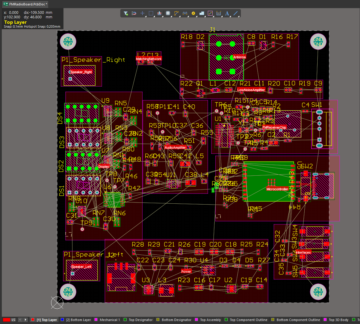
The rooms are the transparent purple boxes and their respective names are shown white text with the red background. When arranging the rooms, don’t worry about the placement of the individual components within each room just yet - try to fit the in the rooms, however, or just move the rooms and not their respective components.
Placing Components
With all the rooms strategically organized, components can now be arranged within the rooms. Components should be placed close to each other while still allowing room for the footprints/pads to be manufacturable and for the components themselves to still be placed down on their footprints manually without hitting other components. It may be helpful to deselect Rooms in Properties->Selection Filter. Keep in the mind the following notes from the lectures regarding component placement:
- Decoupling capacitors should be placed close to the power pins of their respective IC. It’s a good idea to also place a via to GND on the other side of the capacitor.
- Silkscreen reference designators should be visible, only be placed on bare substrate or soldermask (not on exposed copper), and arranged in a such a way that there is understanding as to what footprint the reference designator is referring to.
- Ensure that routing a trace from one component to another can remain smooth and short.
- Air wires (the thin light-colored lines going from one pad to another) show net connections and are useful for telling what component connects to what at a glance.
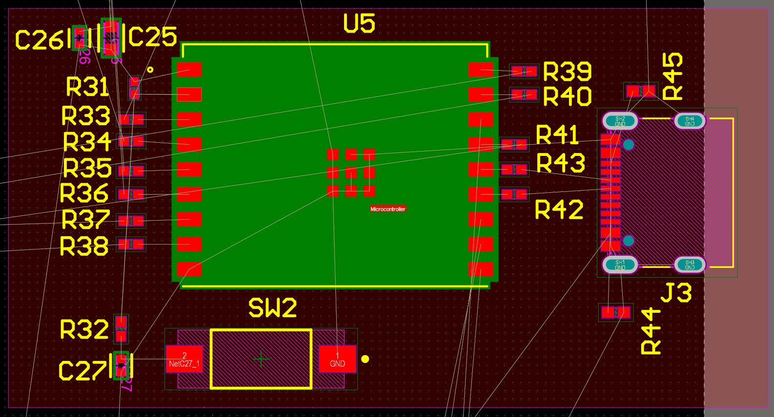
From here on out, you’ll need to determine how your board should be setup, but the layout for the Microcontroller room/sheet will be shown as an example.
Component Routing
Only continue through this section if your schematic has been fully completed and checked by the course staff.
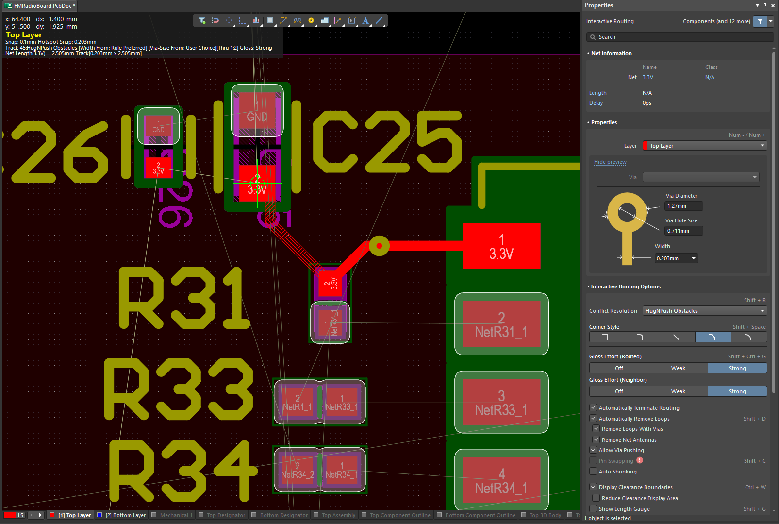
Routing Regular Traces
Use the Interactive Routing tool or CTRL-W to route tracks/traces from pad to pad. You will also be able to change/adjust the track/trace width and cornering style.
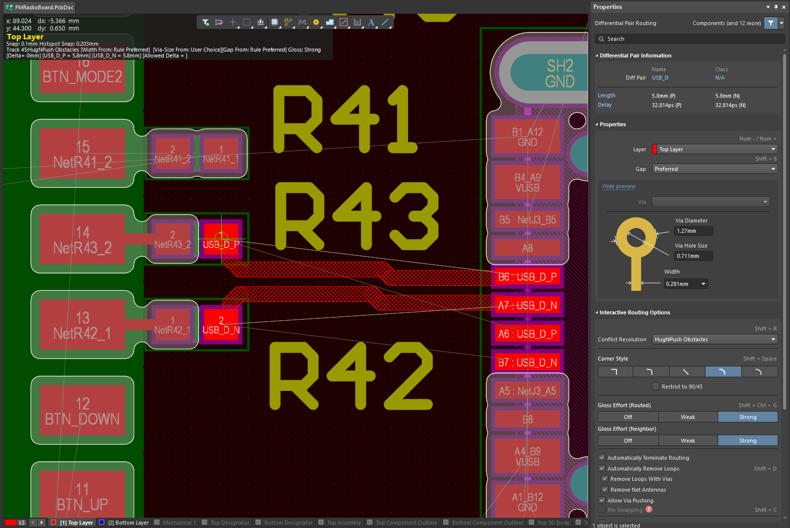
Routing Impedance-Controlled Traces
Using the Interactive Differential Pair tool, the differential USB data lines can be routed while maintaining the 90 Ohm differential impedance that they require. Notice how the gap between and width of the differential pair traces match what was determined in the impedance profile created in the Layer Stack Manager.
Copper Pours
Copper pours are useful nets that connect to a lot of components (such as the GND net). In the case of this board (and in general you may want to do this for most boards), we’ll be conducting a copper pour over the entire board outline on both the top and bottom layers and assigning it to the GND net.
In Altium, we do this via a polygon pour, where the polygon in the board outline. We can create one by selecting Tools->Polygon Pours->Polygon Manager->New Polygon From...->Board Outline
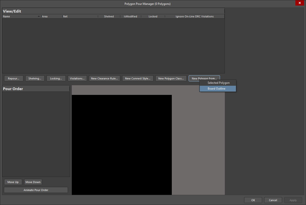
From there, we can assign the board outline polygon pour to be on the top layer along the GND net and to Pour Over All Same Net Objects.
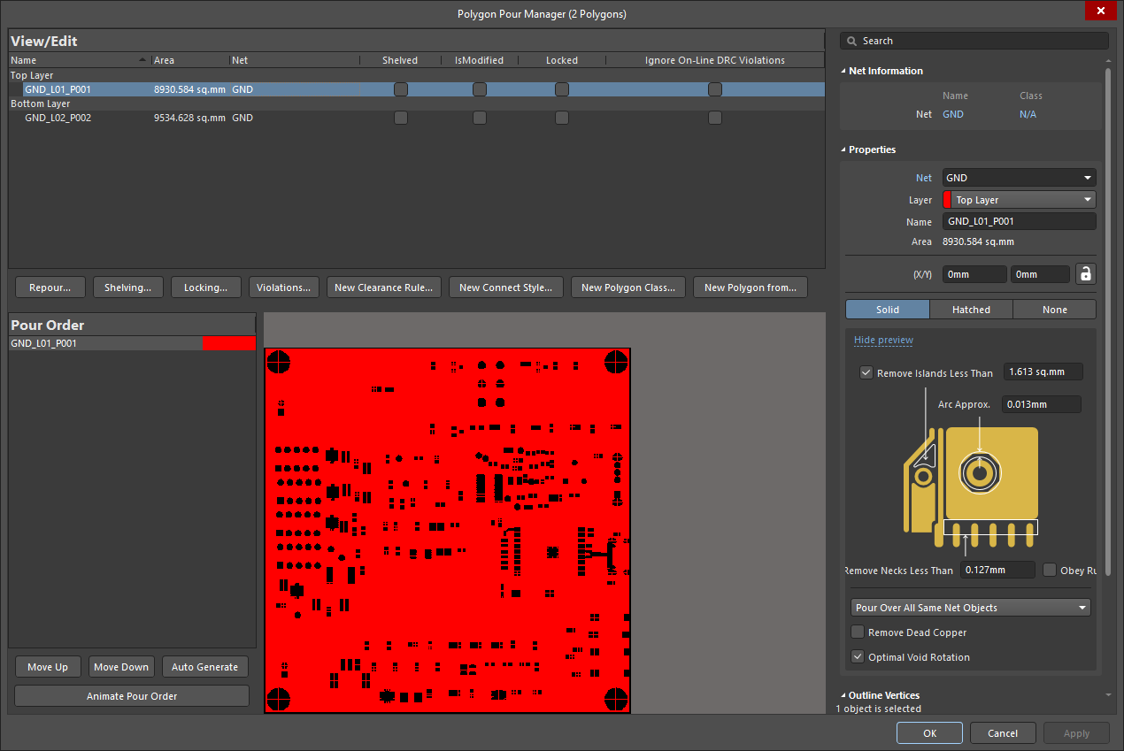
And do the same for the bottom layer.
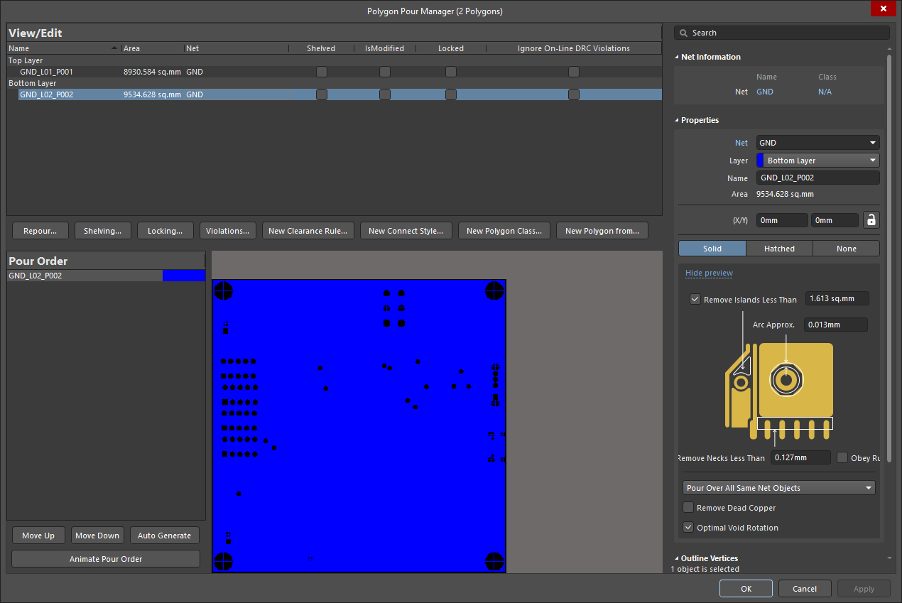
Since polygon pours are static, they will remain unchanged even if traces or components are moved around on the board. Therefore, to update the polygon pour, it must be repoured via the Polygon Pour Manager (see the Repour... option).
On the other hand, since polygon pours often cover large areas with copper, it can be hard to see traces that you have newly routed over where a polygon pour was made.So in order to hide a polygon pour from view (and have it repoured later), the polygon pour can also be shelved (i.e., hidden) via the Polygon Pour Manager by hitting the checkbox under the Shelved column for the polygon pour that should be shelved.
Note that polygon pours can be drawn via Place->Polygon Pour... and doesn’t have to necessarily be the board outline shape. All polygon pours are, however, adjusted via the Polygon Pour Manager.
Conclusion
This concludes the instruction for Lab 05. From here, you should attempt to layout your entire board. In Lab 06, we’ll go over some additional final steps for the board layout including getting it ready for fabrication/purchase, so it’s best to have a finished board by then.
Course staff will be conducting live board reviews and providing feedback during Lab 06. Therefore, please take today and tomorrow to complete the lab as best you can. You can also check out the Resources page page for additional information.
Footnotes
-
OSHPark is a US-based PCB fabricator that focuses on fabricating low-quantity prototype board on a pay-by-board-area rate. They’re potentially a good choice for fabricating one’s personal PCB project due to their low-cost and their domestic production. We won’t be using OSHPark for fabricating the FM radio project PC, but their stackup and fabrication capabiltiies are pretty similar to that of other low-cost fabricators, hence why we use them as reference. ↩
-
Dielectric constant is a synonym for the relative permittivity of some PCB dielectric/substrate material (which is assumed to be linear and isotropic) and is also sometimes abbreviated as
Dk. A similar parameter that is often seen for a dielectric/substrate material is the loss tangent, also known as dissipation factor, $tan(\delta)$ orDf, which determines the amount of attenuation a signal will experience as it propagates through the dielectric/substrate. ↩