’
Finishing up the Schematic
In Lab 03 you be began the arduous process of finishing your schematic for the FM radio, specifically by creating its power regulators and building out its antenna interfaces. In this lab, you’ll continue off of such work and complete schematic sheets for the
- FM radio receiver chip,
- Display, and
- Interfaces.
Along with those, you’ll also complete some miscellaneous tasks meant to complete some unfinished parts of some schematic sheets. Let’s get started!
Warmup
To warmup our minds before delving into the three new schematic sheets, let’s first address the miscellaneous tasks needed to finish up our existing schematic sheets.
Microcontroller Ports
In Lab 01, you placed down the ESP32 onto your Microcontroller sheet. While this is great and all, the ESP32 is not setup to do anything! There are no connections to it (other than to the USB-C connector for flashing and power), making the device quite pointless in our design - so let’s change that.
We’ll need to add ports to our Microcontroller schematic that attach to our ESP32 and provide it interfaces by which to connect to other sheets and control other devices. Specifically, each sheet port we add will need to be connected to a general purpose input/output (GPIO) pin on the ESP32. Each GPIO pin can be configured to read or write digital data or even analog signals.
On the Microcontroller schematic sheet, use the following table to fill in the missing ports. Each row tells you what port to add, it’s basic function, and to which GPIO pin it should connect to on the ESP32. Note: be sure to place a 0-ohm resistor in series with the port label and the pin on the ESP32 (that way we can severe net connections easily for debugging).
| Sheet Port Name | ESP32 GPIO pin | Function | Connection |
|---|---|---|---|
RST_OUT |
IO4 | Turns off/on or resets | FMReceiverChip |
IRQ_IN |
IO5 | Allows interrupt of ESP32 processing | FMReceiverChip |
I2C_SDCLK |
IO6 | I2C clock line | FMReceiverChip |
I2C_SDIO |
IO7 | I2C data line | FMReceiverChip |
REG_CLR |
IO8 | Clears shift register | Display |
REG_LE |
IO9 | Clocks storage register | Display |
BTN_MODE1 |
IO10 | Mode 1 button | Interfaces |
BTN_UP |
IO20/RXD | Up button | Interfaces |
BTN_DOWN |
IO21/TXD | Down button | Interfaces |
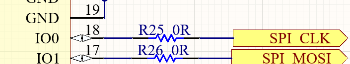
SPI_CLK |
IO0 | Shift register clock | Display |
SPI_MOSI |
IO1 | Shift register data | Display |
BTN_MODE2 |
IO2 | Mode 2 button | Interfaces |
SPI_CE |
IO3 | Output enable | Display |
Once you have all these ports attached to the ESP32 (via 0-ohm resistors), be sure to update your top-level schematic sheet entry for Microcontroller to have the ports you just added.
Removing Display Driver
In order to simplify your schematic capture, we’ll combine the DisplayDriver and Display sheets.
What this means for now is that you should delete your DisplayDriver sheet as well as its sheet entry in the top-level schematic sheet
Adding Speakers
For our two stereo speakers, we’ll be using the CMS-30204-18L250, which can mounted to our PCB and connects using a convenient JST-style connector.
What this means for us is that in order to be able to connect to our speaker, we need to add its corresponding JST-style header to our Speaker sheet. You can do so by placing the S2B-XH-A part on the Speaker sheet and attaching pin 1 to AUDIO_IN and pin 2 to GND.
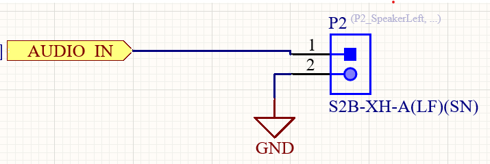
Also, keep in mind that on the top-level schematic, our two Speaker sheet entry instances will need unique reference designators so that Altium can distinguish between them.
Audio Amplifier Consolidation
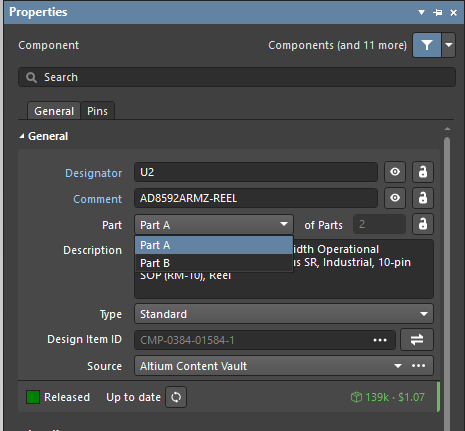
In Lab 02, you designed an audio amplifier and placed it your AudioAmplifier sheet. In doing so, you used the AD8592 operational amplifier, which actually consists of two opamps co-located on a single chip. This means that when we place the AD8592 onto our schematic and we’d like to use both of its opamps, we have to use a multi-part symbol that specifies the two integrated opamps and that they belong to the same package. This is to ensure we don’t instead end up placing two separate AD8592s and use only one opamp from each.
Multi-part symbols give us the least trouble when each of their instances exist on the same sheet. That means we’ll consolidate our AudioAmplifier sheets into a single one with two inputs and two outputs for the left and right audio channels. Do so by ensuring that there is only one AudioAmplifier sheet on the top-level schematic.
Afterwards, duplicate the audio amplifier you put into the AudioAmplifier sheet and change the amplifiers’ ports to AUDIO_IN_L/AUDIO_OUT_L for one amplifier and AUDIO_IN_R/AUDIO_OUT_R for the other amplifier.
Now, we need to make sure that the two opamps (in the left and right amplifier channels) end up being selected from the same AD8592 package using a multi-part component. To do this, first ensure that both opamps have the same reference designator. Afterwards, open up the properties for the each of the opamps and ensure one is assigned to be part A and the other is assigned to being part B.
Altium
KiCad
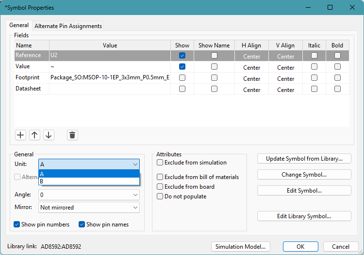
You should then end up having two opamps on your AudioAmplifier sheet with identical reference designators - except one has an A and the other has a B (e.g., U2A and U2B). You should also notice that some of the pin numbers between the two amplifiers should be different (since each opamp uses a different part of the AD8592 package).
Once you have finished these change, be sure to update your top-level schematic sheet entry for AudioAmplifier (now there should be only one) to have the ports you just added.
Checklist
Just to be sure that we’ve addressed all of the unfinished issues with our schematic, below is a checklist of the schematic parts we should have finished:
- Removing the
DisplayDriversheet. - Adding ports to the
Microcontrollersheet. - Add speaker connectors to the
Speakersheet. - Consolidate the two
AudioAmplifiersheets and implement a multi-part component.
FM Radio Receiver Chip
Arguably the most important component to lay down onto the schematic, is the FM radio receiver chip itself. Since the chip takes care of most of the radio and audio processing, putting on the schematic only involves adding some of its peripheral devices as well as attaching ports.
As pulled from the application circuit, implement the following schematic into your FMReceiverChip sheet. For the potentiometer, use the PTV09A-4020U-B104 part.
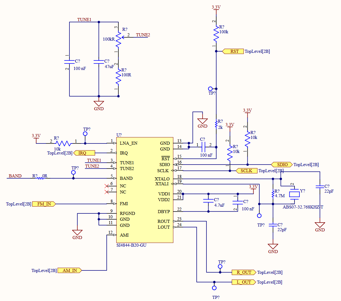
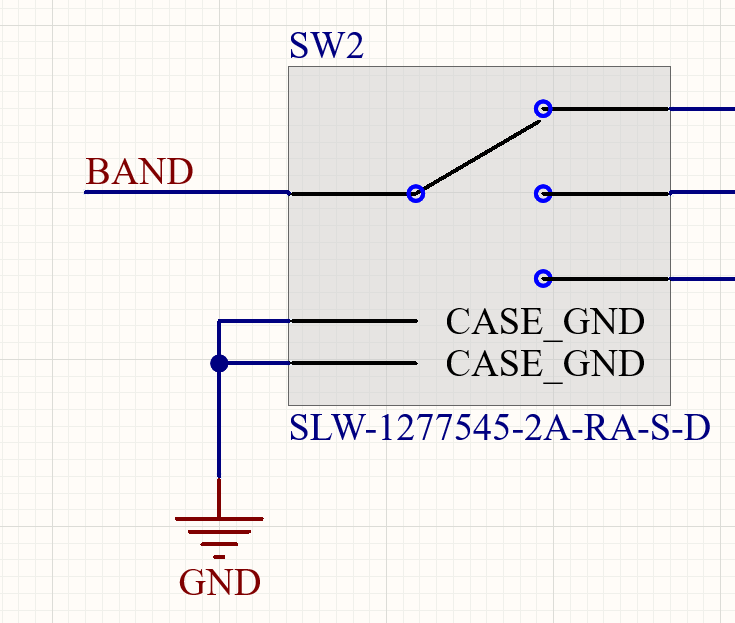
Notice how the BAND net leads nowhere? That’s because it’s supposed to connect to a switch that will allow for band selection. Using the SLW-1277545-2A-RA-S-D SP3T switch, attach the BAND net to center pole of the switch then determine the circuit configuration of the switch necessary to allow for AM/FM band selection in the U.S. as well as the ability to select having the FM radio receiver chip to be controlled a microcontroller - as described in different parts of AN602: Si4822/26/27/40/44 Antenna, Schematic, Layout, and Design Guidelines.
Once you fill up your FMReceiverChip schematic sheet correctly, be sure to update your top-level schematic sheet entry with any ports created in the lower sheet.
Interfaces
Let’s put our interfaces so that we can actually interact with our radio.
In the Interfaces schematic sheet, place four pushbuttons (use the 1437566-3 part) and assign them to the BTN_UP, BTN_DOWN, BTN_MODE1, and BTN_MODE2 port such that when a pushbutton is depressed its corresponding port is shunted to GND. Additionally, attach a 1 uF bypass capacitor (to help with de-bouncing) to each of the pushbuttons and their respective ports.
Once you have finished the Interfaces schematic sheet correctly, be sure to update your top-level schematic sheet entry with any ports created in the lower sheet.
Display
Background
The display consists of four 7-segment displays colocated to each other in a line. They will be able to display the current tuned frequency (e.g., 101.5 MHz) as well as other information.
In order to reduce the number of GPIO pins required to control the four 7-segment displays, a shift register can be assigned to each 7-segment display and used to shift in values to be displayed. The shift register used is the SN74AC595, which consists of
- a serial-in parallel-out (SIPO) shift register (to control shifting new instructions into the display),
- a parallel-in, parallel out (PIPO) storage register (which latches the value from the SIPO register to the output), and finally
- an output buffer, which is used to instantaneously control whether the display is on or off.
With these features, the SN74AC595 can be directly connected to a 7-segment display and control what is being statically displayed, as well as change it instantly when a new value is shifted in.
However, in order to provide enough current to drive all the LEDs in the 7-segment displays, the SN74AC595 must be configured to operate off 5.0V, which poses an issue with communicating with the ESP32, which operates on 3.3V, due to unequal logic levels.
Level Shifter
To allow for the ESP32 to effectively communicate with the shift registers, we can use a level shifter to convert the 3.3V-logic used by the ESP32 to the 5.0V-logic level used by the the shift register.
Using the SN74LV8T541 unidirectional level shifter, set up your level shifter to convert the ESP32’s 3.3V logic input/output (I/O) logic to 5V I/O logic that the shift registers can understand within your Display schematic sheet.
As a hint, the photo below shows the inputs and corresponding outputs that your level shifter should have.
If you recall back to the ports we set up in the Microcontroller sheet, we are creating ports that will allow us to connect to the ports on the microcontroller crucial to communicating with the display.
Shift Register and LEDs
Focusing back towards the SN74AC595 shift registers, its 8 outputs will each connect to an LED on a 7-segment display to control it. However, the current on each output cannot exceed 10 mA without causing undesired behavior or damage. Using the datasheet for the common-anode 7-segment display, INND-TS30RAB, determine the series resistance needed between an output of the SN74AC595 shifter register and an LED in the 7-segment display such that 10 mA flows. Assume that the maximum voltage output of the SN74AC595 is 5V.
After determining the series resistance, use a corresponding resistor array to connect the output of a SN74AC595 shifter register to an INND-TS30RAB 7-segment display. Do not use individual resistors for this (it’ll help us save on parts). In KiCad, you can use the R_Pack04 symbol. In Altium, there are a few options in the library that you can choose from which have names starting with “EXB”. When you have finished this step, you can copy-paste it three additional times to get the four total digits needed.
Wiring up the Shift Registers
Using the 5V-logic nets created using the level shifter, wire each of the four shift register and 7-segment display combinations together such that the ESP32 can load a 32-bit word into the display and display it as a four digit number (and clear and update it as needed). It’s recommended that you check the datasheet for the SN74AC595 for hints on doing this.
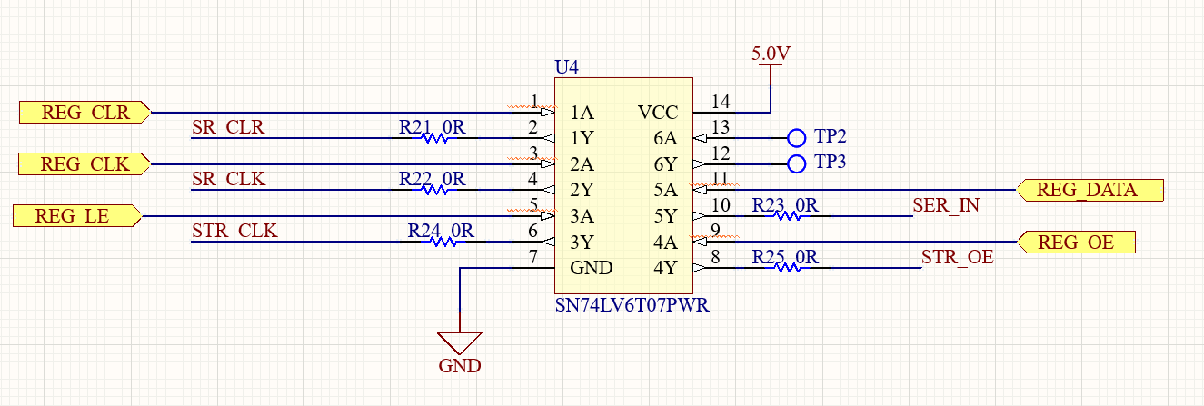
Below describes the 5V-logic nets in greater detail to help with determining where such nets should connect to. As a quick note, SR refers the SIPO shift register part of the SN74AC595 and STR refers to the PIPO register used to latch the output.
| 5V-logic Net | Function | Part of SN74AC595 |
|---|---|---|
SR_CLR |
Clears stored values | SIPO Shift Register |
SR_CLK |
Clock signal | SIPO Shift Register |
STR_CLK |
Clock signal | PIPO Register |
SER_IN |
Serial data input | SIPO Shift Register |
STR_OE |
Output enable | Output Buffer |
Changing Sheet size
The standard sheet will likely be too small to fit all of the display driver pieces on. We can just expand the sheet size to accommodate our needs.
In KiCad, click on Page Settings towards the left of the top toolbar. Now, change the paper size to something larger (like 11x17in).
In Altium, open the Properties panel when you have nothing selected. Go down to the “Page Options” section and select a larger sheet size (like 11x17in).
Summary
Once you have finished up the previous blocks, you just need to properly connect them together on the top-level schematic.
But once that’s done, congrats! You have just created the schematic for a multi-band radio receiver. Save and upload your work (just PCB project files, LTspice files not needed) by:
-
Altium users: be sure to select
Save to Serverin the Projects Manager toolbar so that your work is uploaded to the course’s Altium workspace! -
KiCad users: be sure to save to commit to main and push to origin so that your local changes get saved to your GitHub repository!
Please do so by midnight so that course staff can grade your work.