Introduction
This lab is the first of two labs where you’ll be placing into schematic all of the components that make up the FM radio. A lot of this lab will utilize skills you previously learned, such as reading over datasheets, utilizing manufacturer application circuits, and designing circuits using SPICE simulation. You’ll apply these skills block by block to fill in each major section of the FM radio’s system diagram (e.g., amplifier, display, power regulator) then define the input/output interfaces needed to connect each block together.
EDA Setup Note
Both KiCad and Altium users should continue using the parts provided in lab 1. For KiCad users, this is the FMRadioParts symbol library For Altium users, these are the components found in the workspace component library.
Power Regulators
The first block we’ll tackle are the power regulators. It’s arguably the most important part - since how are we to turn on our devices without any power? Recall from Lecture and Recitation 04 how it was determined that we only needed two regulators to achieve the FM radio’s power needs:
- A 5.0 V output buck-boost converter that should be rated for >1A of output current.
- A 3.3 V output LDO regulator that should be rated for >0.5A of output current.
Providing the actual power to board are two options:
- 5V 1A regulated power from a USB 2.0 connection over USB-C.
- 6V external battery pack consisting of 4xAA batteries.
Since there is always the possibility that a user could try to plug both potential power sources into the board and in doing so potentially fry the USB host, batteries, or the board itself, we’ll need to integrate a multiplexing switch that will prevent both input sources from trying to power the FM radio at the same time and rather selecting a preferred device (USB input) to act as the sole power source.
5V Buck-Boost Converter
We’ll use the Texax Instruments TPS63060 as our integrated 5V buck-boost converter.
Open up the datasheet and check that the specifications for the DC-DC converter meet our power requirements for the 5V net.
| Criteria | Value | Unit |
|---|---|---|
| Output Voltage | 5 | V |
| Output Current | >1 | A |
| Max Input Voltage | >6 | V |
| Min Input Voltage | <4.5 | V |
After you’ve made the check, use the regulator’s typical application circuit to create a 5V buck-boost regulator in your Power schematic sheet. As you go through this, be sure to note:
- Use the
IHLP1616ABER1R0M011 uH power inductor across theL1andL2pins of the regulator - Assign the global power net
BATTto the voltage input pin(s) of the regulator. - Assign the global power net
5V_BATTto the voltage output pin(s) of the regulator.
3.3V Linear Regulator
We’ll use the AP2112K-3.3TRG1 as our integrated 3.3V low-noise, linear amplifier.
Open up the datasheet and check that the specifications for the LDO meet our power requirements for the 3.3V net.
| Criteria | Value | Unit |
|---|---|---|
| Output Voltage | 3.3 | V |
| Output Current | >0.5 | A |
| Max Input Voltage | >6 | V |
| Min Input Voltage | <4.5 | V |
After you’ve made the check, use the regulator’s typical application circuit to create a 3.3 Linear regulator in your Power schematic sheet. As you go through this, be sure to note:
- Assign the global power net
5.0Vto the voltage input pin(s) of the regulator. - Assign the global power net
3.3Vto the voltage output pin(s) of the regulator.
We’ll essentially be attaching this 3.3V LDO regulator to the output of the 5V regulator to provide extra stability.
Status LEDs
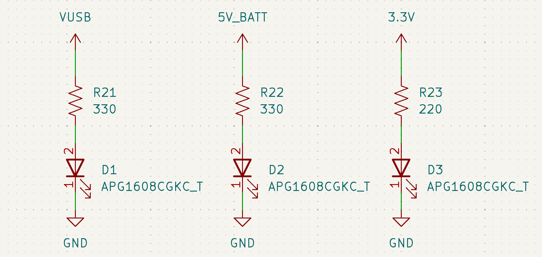
Attach some LEDs as shown below to allow us indication of which nets are working and receiving power
Battery Connector
Finally, add in a terminal block that we can connect to a battery pack. Use the 691411510002 symbol for this.
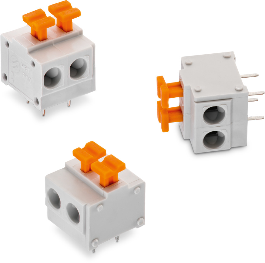
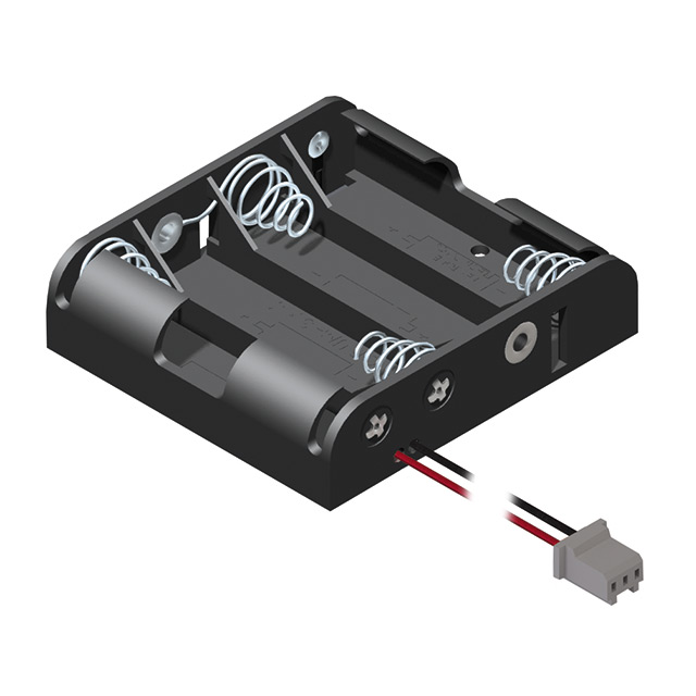
This terminal block will allow us to attach any 4xAA battery pack to the PCB. Keep in mind the following:
- Pin 1 of the connector should attach to a
BATTglobal power net. - Pin 2 of the connector should attach to
GND.
Power Multiplexer
As mentioned previously, given that we have two potential voltage supplies, USB and battery power, we need a controller that can switch to using the supply that is available and to choose a supply if both of them are available at the same time.
We’ll use the TPS2115A power multiplexer. Using the datasheet, implement the device as recommended for the typical application circuit involving auto-switching between dual power supplies. As you go through this, be sure to note:
- Input 1 should be attached to the
VUSBglobal power net. - Input 2 should be attached to the
5V_BATTglobal power net. - The output should be attached to the
5.0Vglobal power net - The current limit of the multiplexer should be set to approximately 2 A (hint: a current limit resistor must be set).
- You can disregard any connections to the
STATpin of theTPS2115Aand just leave it floating. - The load capacitance
C_Lfor the regulator should be 10 uF.
Radio
The FM receiver chip abstracts away much of the complex RF circuitry needed to receive and demodulate radio signals, so we only need to follow the manufacturer’s recommendations for how the FM receiver chip should be configured in the schematic.
The FM receiver chip that we are using is the Si4844-B20. It contains functionality that allows for the radio to be analog-tuned via a potentiometer, but also has a digital interface via I2C that allows for a microcontroller to configure the chip. Features such as volume, band selection, and receiver optimizations can be configured digitally.
The radio receiver in the chip itself actually support 2 other modulation types, in addition the FM that we have been focusing on. It has the ability to receive analog modulation (AM) radio as well as shortwave (SW) radio. We want to activate all three of these receive modes, so we’ll have to do some special configurations of the receiver in the schematic.
We’ll start off building the RF frontend (i.e., the circuits between the antenna and the receiver chip).
RF Amplifier
The RF amplifier in our radio is not actually intended for the FM receiver, which is able to do amplification at FM frequencies (~100MHz) via on-chip amplifiers. The separate RF amplifier is actually intended for the SW receiver since such signals are usually be received from very far-distanced transmitters (think other continents entirely). Shortwave radio is a very popular means by which individuals listen to broadcasts across the world, since the radio waves are given a range boost by virtue of being able to be guided on the Earths ionosphere around the planet.
To implement the RF amplifier, you’ll need to do a little bit of design. As mentioned in Lecture 03, we’re going to a BJT common-emitter amplifier topology in order to achieve high gain - crucial for the SW signals which will be very weak but also very narrowband. The transistor we’ll use is the 2SC3356, which is an NPN BJT with low noise and high gain.
Open up LTspice and replicate the BJT common-emitter amplifier circuit below. V2 and R6 represent the Thevenin equivalent circuit to our receiver’s SW antenna (which will receive a very small voltage from the SW radio wave and have an impedance of 75 Ohms). L1 and C3 form an impedance matching network that converts the 75-Ohm impedance of the antenna to the high input impedance of the BJT Q1. Finally, R5 represents the RF input of the FM receiver chip, which has an input impedance of 10 kOhms.
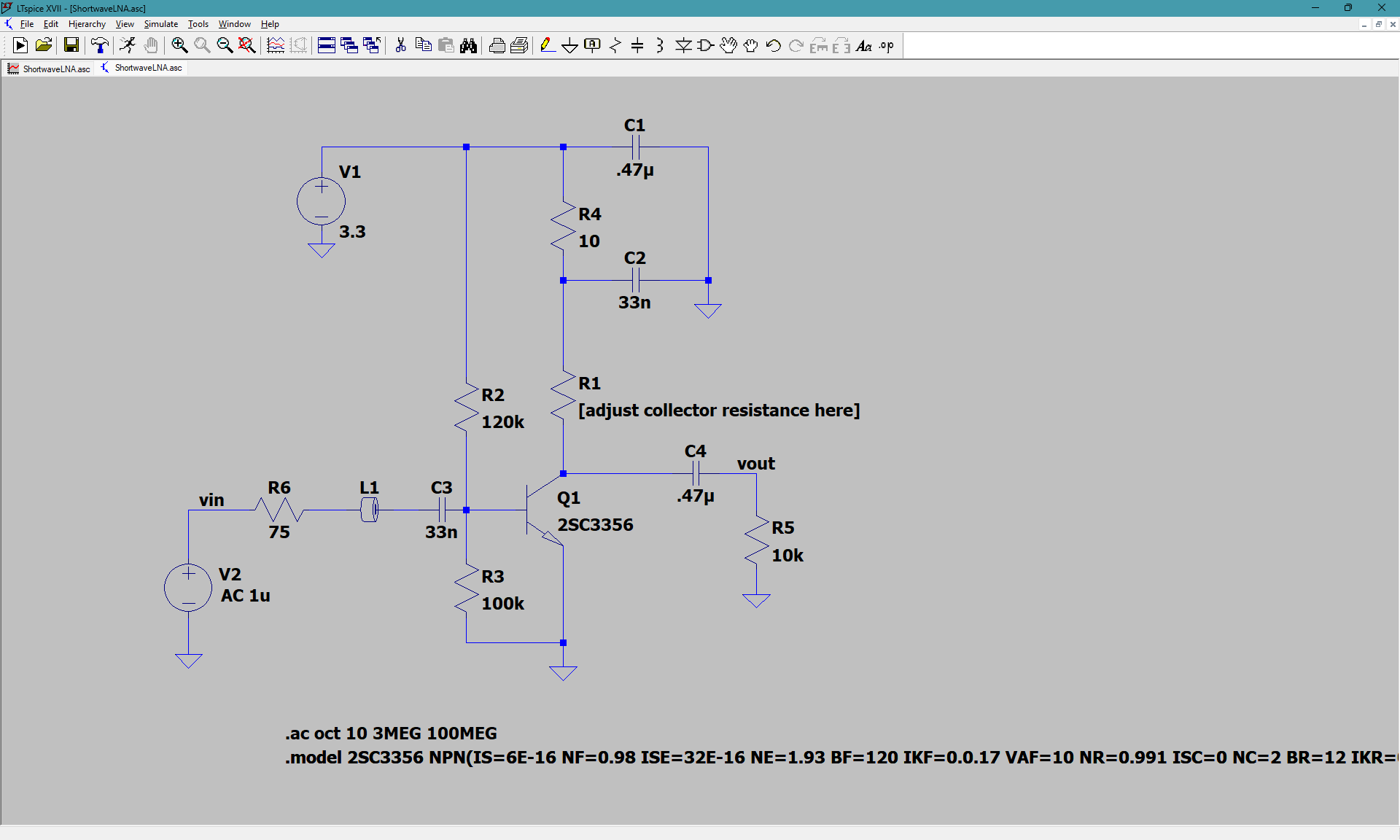
Keep in mind some important notes while doing so:
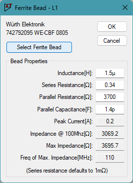
- For the ferrite bead,
L1, select theWurth Elektronik 742792095.
-
For the NPN transistor, place down an
npncomponent then right-click the “npn” label text next to the symbol and replace it with “2SC3356” such that it visually matches the above schematic (the2SC3356is not available to be selected in thenpncomponent’sPick New Transistordropdown menu so we need to import its model). -
For the BJT’s
.model 2SC3356 NPN(...)model SPICE directive, copy-paste the following:
.model 2SC3356 NPN(IS=6E-16 NF=0.98 ISE=32E-16 NE=1.93 BF=120 IKF=0.17 VAF=10 NR=0.991 ISC=0 NC=2 BR=12 IKR=0.17 VAR=3.9 RB=4.16 IRB=1.96E-04 RBM=3.6 RE=0.38 RC=2 XTB=0 EG=1.11 XTI=3 CJE=2.8E-12 VJE=1.3 MJE=0.5 TF=15E-12 XTF=6 VTF=10 ITF=0.2 PTF=0 CJC=1.1E-12 VJC=0.7 MJC=0.55 XCJC=0.3 TR=1E-09 CJS=0 VJS=0.75 MJS=0 FC=0.5 Vceo=12 Icrating=100m mfg=cel)
With the whole RF amplifier circuit in LTspice, determine a value for the collector resistor, R1, such that a voltage gain of at least 30 dB is achieved from 10 MHz to 30 MHz. (hint: to view the gain in an AC simulation, plot V(vout)/V(vin), which shows the voltage ratio between the vin and vout nets in the LTspice circuit).
Once your simulation meets the RF amplifier specifications, go ahead and transfer your LTspice circuit into your PCB EDA software (i.e., KiCad or Altium). Be sure to keep the following in mind:
- Do not include
V2,R6, orR5as they’re only meant to represent certain parameters in simulation. V1should be replaced with a3.3Vglobal power net.- Be sure to connect the
RF_INandRF_OUTports of your amplifier schematic sheet to the amplifier itself. - Do not directly import your LTspice design files into Altium/KiCad. Doing so will use the incorrect symbols and just look wrong in general. You should place down components manually within your Altium/KiCad schematic sheets (from the libraries provided) and add wires/nets manually.
Matching Network
Within the MatchingNetwork schematic sheet, create an L-C matching network based off the manufacturer recommended circuit in the FM receiver chip’s application note: AN602: Si4822/26/27/40/44 Antenna, Schematic, Layout, and Design Guidelines.
(hint: look for an L-C circuit going from the FM/SW antenna to the FM input on the receiver chip)
Antenna Schematic
As a final measure, connect up your Antenna schematic sheet as follows:
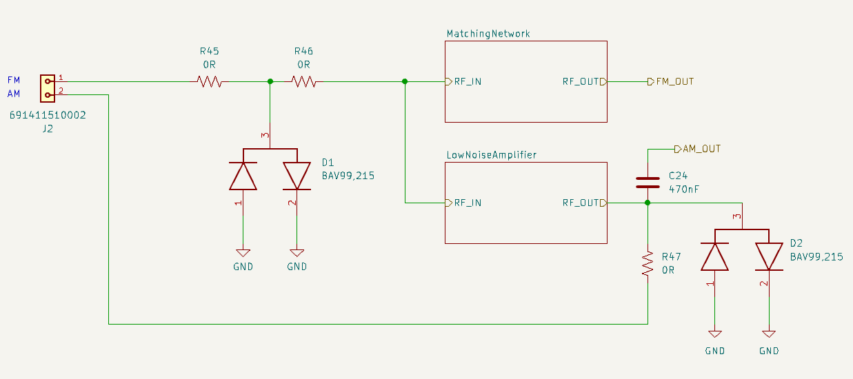
You will need to modify/add the FM_OUT and AM_OUT ports, then synchronize those pins to the schematic symbol on the top level. If you need, refer back to Lab 1 for instructions on how to do that.
Annotate Schematics
As a final step, we are going to annotate our schematics. From here on, we will do this at the end of every lab.This process lets us set/reset the reference designators for our parts.
Altium
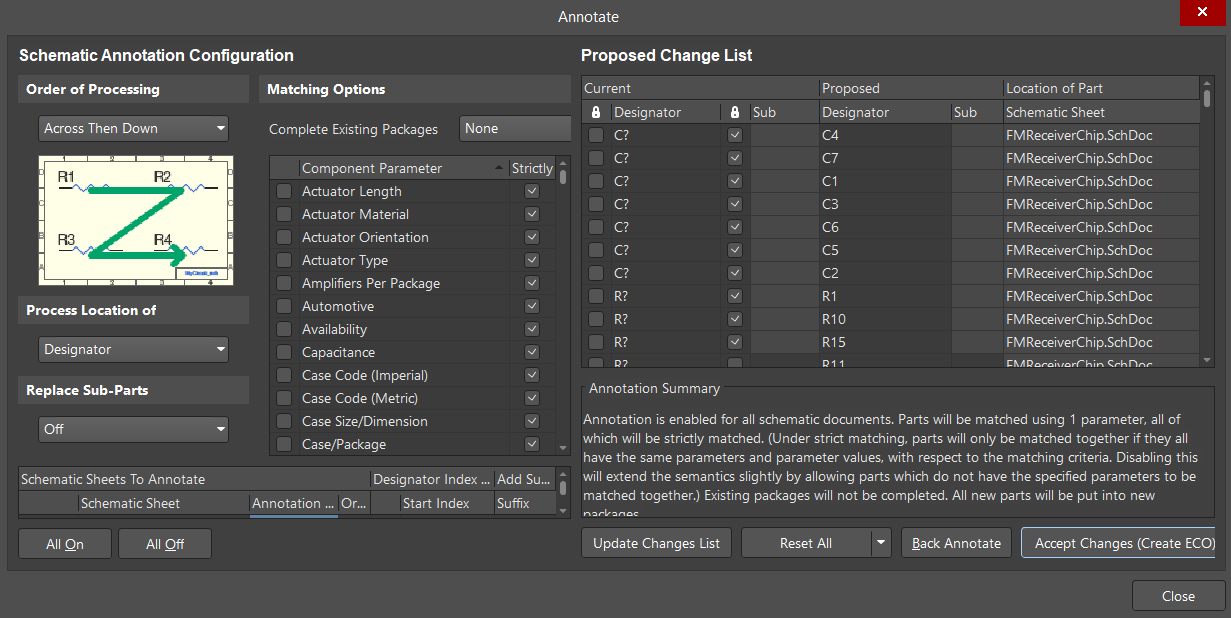
First, double check that all of your reference designators follow the format [A-Z][A-Z][1-100]. You can do this by going to Tools > Annotation > Annotate Schematics. All of your reference designators should be formatted as one or two letters followed by a number or a “?”. If any of them aren’t you’ll have to find this part and manually change the format in properties.
Now, we can annotate the whole schematic. Go to Tools > Annotation > Annotate Schematics. The defaults should be fine for now. Hit Update Changes List then Accept Changes (Create ECO). In the ECO (Engineering Change Order) dialog, hit Execute Changes. Now all of your parts should be annotated.
KiCad
You might not need to do anything with the annotation in KiCad, since it automatically sets designators as you place parts. However, it can help to clean them up in case you deleted parts and now have non-sequential designators (i.e R1, R2, R4 but no R3).
First, double check that all of your reference designators follow the format [A-Z][A-Z][1-100]. You can do this by going to Tools > Edit Symbol Fields. All of your reference designators should be formatted as one or two letters followed by a number.
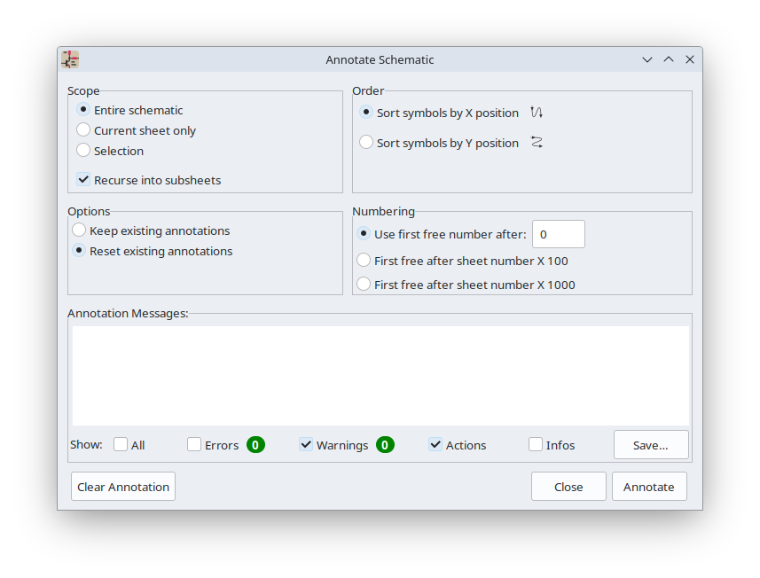
Now, we can annotate the whole schematic. This part is a bit more optional for KiCad users. Go to Tools > Annotate Schematic. If you want to fix any non-sequential designator issues, make sure to hit the “Reset existing annotations” option. Hit Annotate and the tool will take care of everything for you.
Summary
Now, you’re all finished! You just designed and implemented the RF amplifier and antenna matching network for your FM radio and implemented it into your PCB schematic. Save and upload your work (just PCB project files, LTspice files not needed) by:
-
Altium users: be sure to select
Save to Serverin the Projects Manager toolbar so that your work is uploaded to the course’s Altium workspace! -
KiCad users: be sure to save to commit to main and push to origin so that your local changes get saved to your GitHub repository!
Please do so by midnight so that course staff can grade your work.
