Mounting Methods
Surface Mount Technology (SMT)
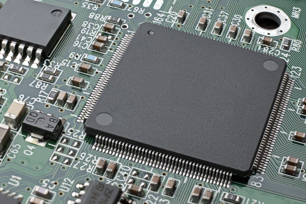
Surface Mount Components are designed to mount onto planar board. They are designed such that their contacts mount directly to flat pads on a PCB. Notice that how on the board photo below components are soldered on the same side that they are mounted on.
Plated Through Hole (PTH)
Plated Through Hole devices are typically what one typically what one thinks about when it comes to electronic components. These devices have metal legs that are designed to be “plugged” into a board and soldered down. The hole is plated to allow it to connect to traces and other devices on the board. In the modern days of ever so compact PCBs, you will often still see PTH components being used for advantages:
- Ease of use
- High power handling
- Simpler to debug
- Able to connect to multiple layers on a board
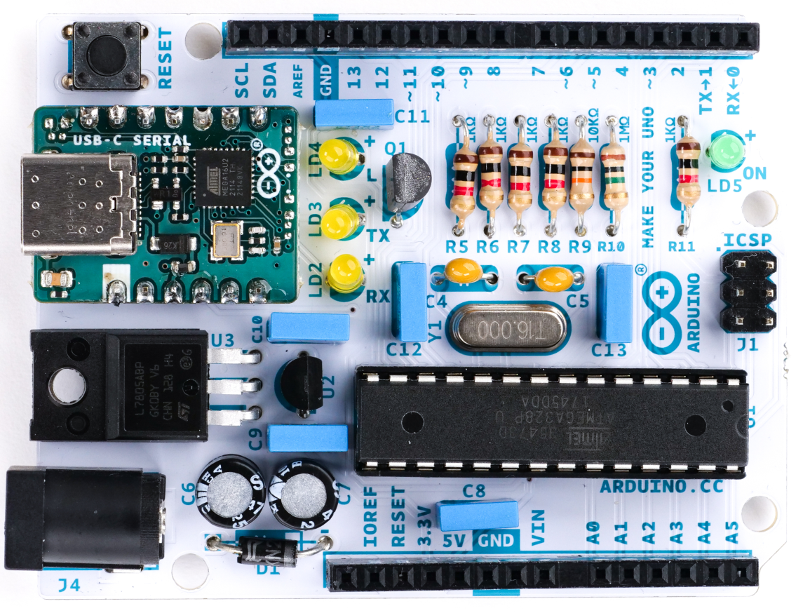
Top view of a through-hole version of the Arduino Uno. Image credit: Arduino
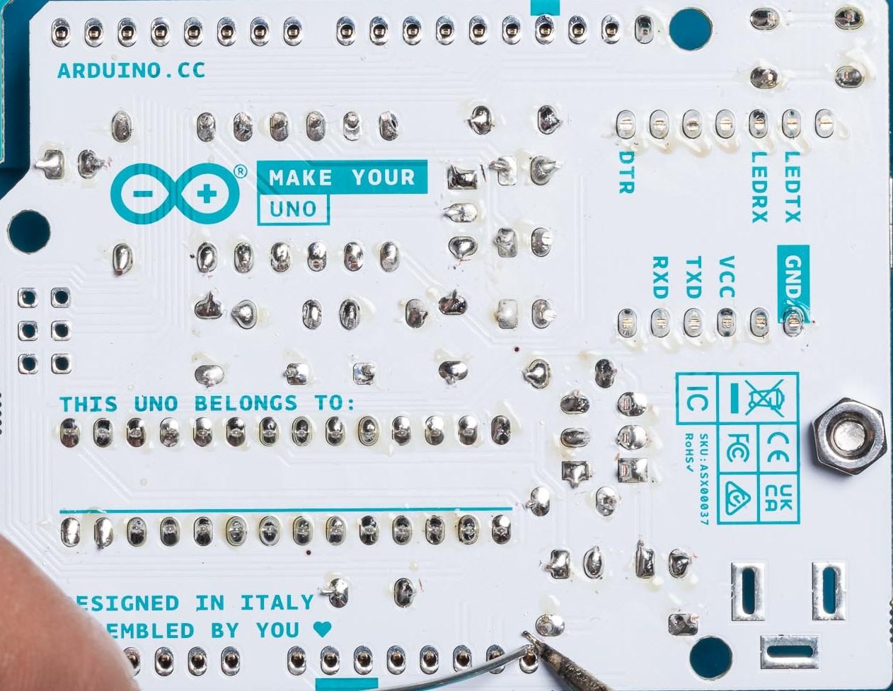
Bottom view of a through-hole version of the Arduino Uno. Source: Arduino
Package Naming
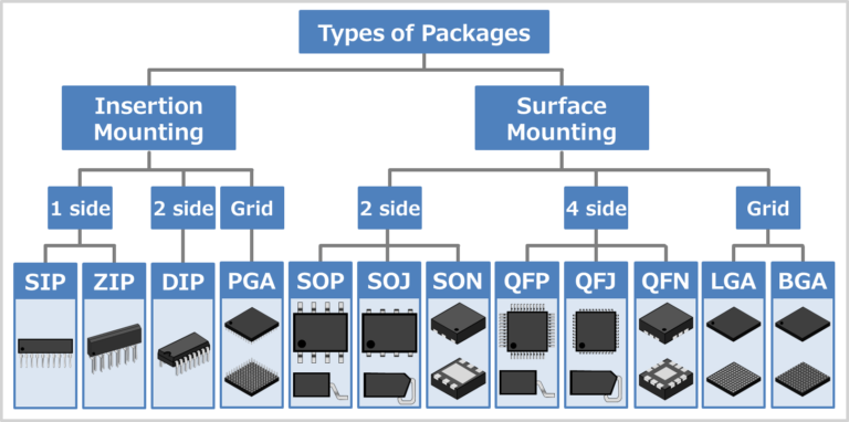
Source: https://electrical-information.com/package-types/
Components (in particular SMT components) come in all sorts of names to describe the way they are manufactured and interacted with. This website provides a pretty good guide. You will likely want to head over there to determine what footprint your device looks the most like, then you can head back here and where we will talk about part naming in KiCad and Altium. The most common one SMT parts are often:
Also not mentioned are:
While SMT components will typically come in these standardized package names, often manufacturers will have different package sizings and layout requirements. Be sure to check a parts datasheet for how its exact dimensions and recommended layout.
Please don’t use LGA/BGA devices in this course. We don’t have the X-ray equipment needed to debug solder joints that are under an IC. If you’re working in industry you’ll get plenty of time to use them. For now, let’s go with a package that we can identify solder joints with our eyes.
Guide for footprint assignment - KiCad
You will want to familiarize yourself with the KiCad footprint naming conventions. Once you know these few things you should be able to find a package fairly quickly.
- Package Name
- Pin Pitch
- Pin Count
Lab 01 for KiCad users describes how to create/add symbols and footprints.
Guide for footprint assignment - Altium
In Altium, each physical electronic device and its variations that can be placed on a PCB (e.g., a 10k resistor, ESP32, or SMA connector) is represented as a “component” which in itself contains both a symbol (for the schematic) and a footprint (for the PCB). An efficent design workflow relies on the existence of accurate and detailed components
Altium provides three different methods for storing components and their links to symbols and footprints:
- File-based integrated library
- Database library
- Altium 365 workspace library
This guide will show you how to make footprint assignments in filed-based integrated libraries, but the process is similar for the latter two.
To start off, let us select a component to use in our PCB design project, in this case we will choose the MIT364-4 chip - it is a common distance measuring IC, though its uses and inner workings are not necessary for this guide. The chip comes in a 20-pin 5x5mm QFN package as shown below.
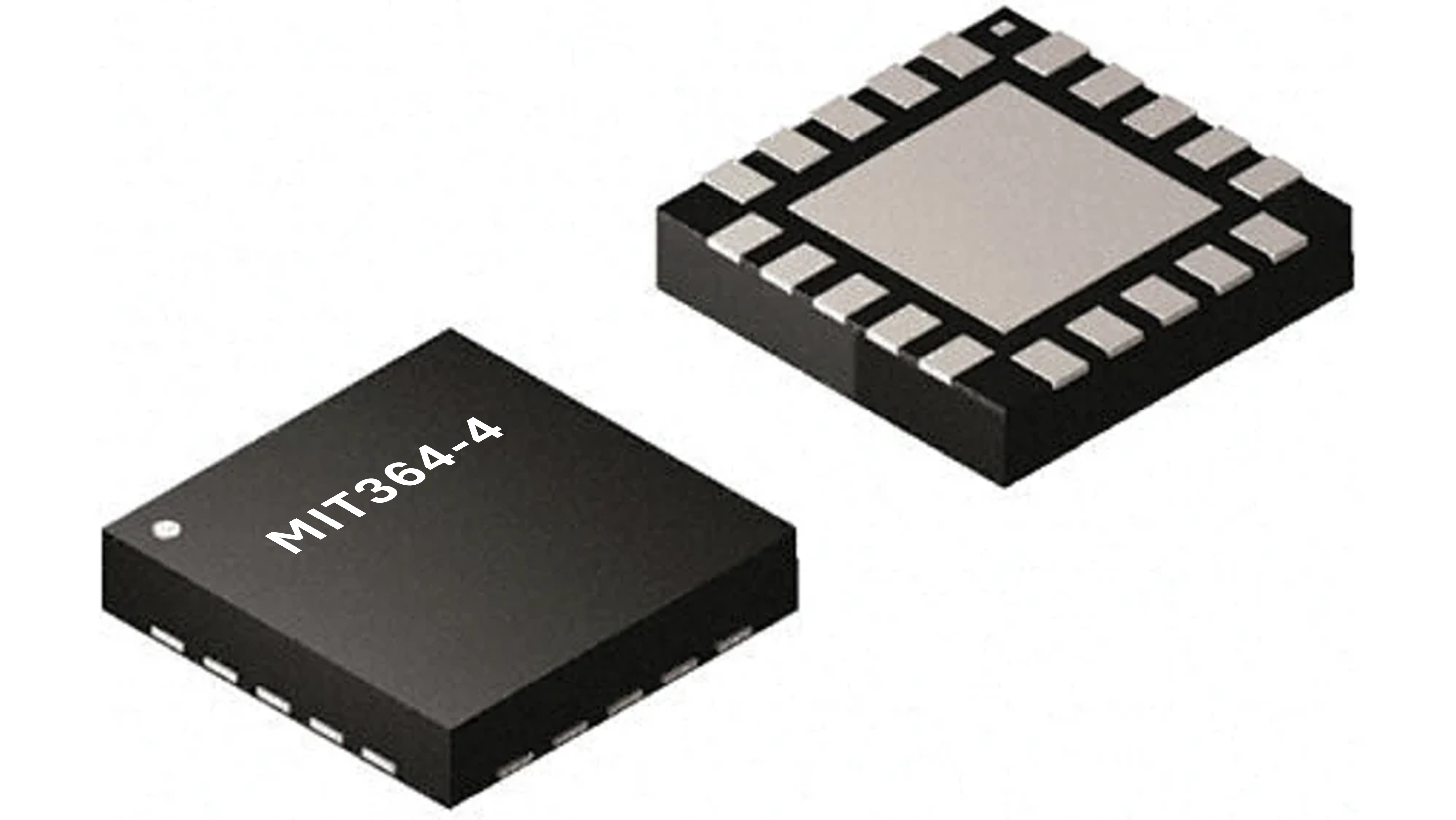 MIT364-4 20-pin 5x5mm QFN package
To start off footprint assignment from scratch, add a new PCB library to your project
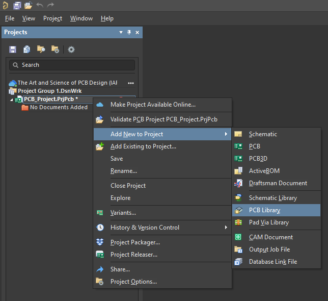
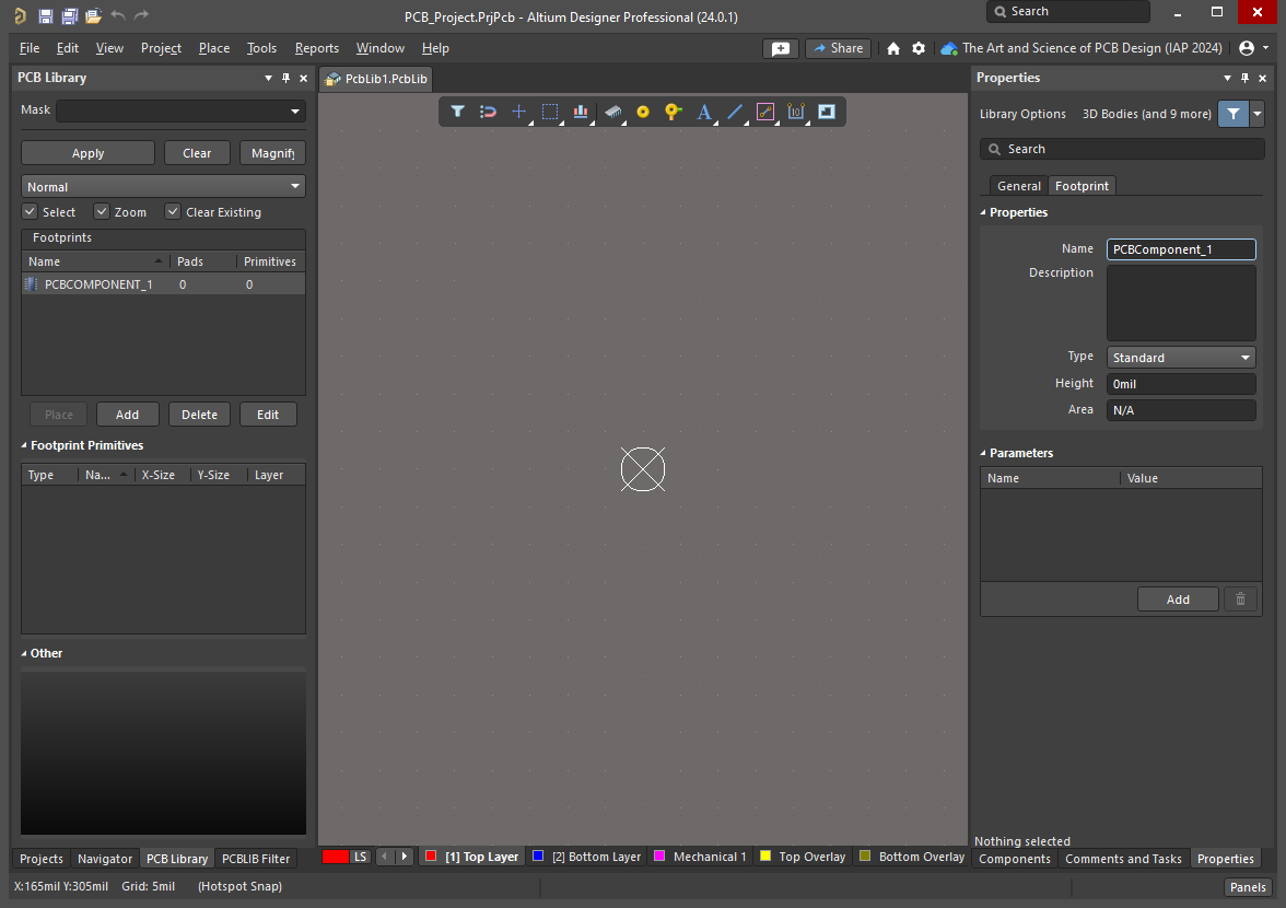
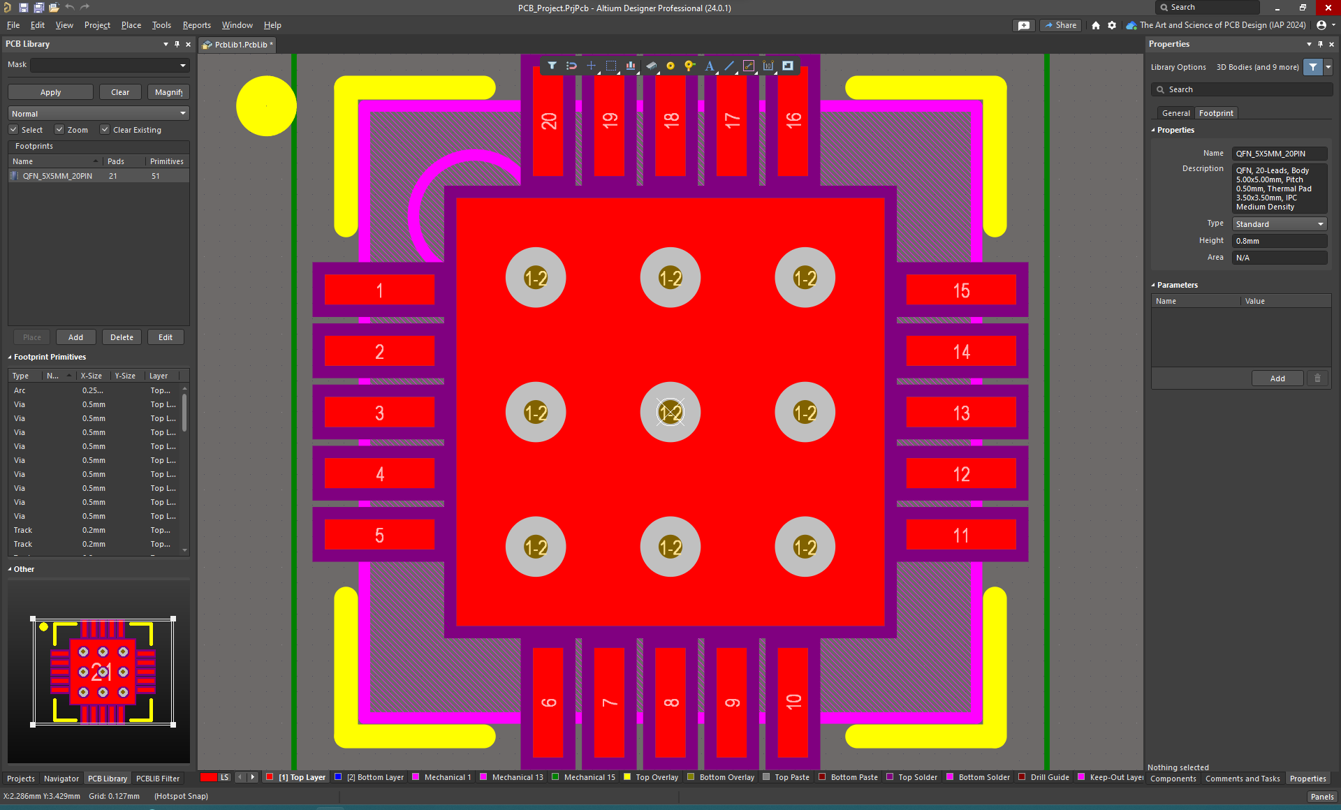
Now we can begin to create our footprints. Within the PCB Library panel (shown below on the left), we can add new footprints and add attributes via the Properties panel (shown below on the right). Finally, we are provided some basic layout tools to create our footprint (shown below in the center).
In the case of our MIT364-4 chip, looking at the datasheet, we created the footprint by hand - but we could have also imported a footprint provided by the manufacturer if available.
In addition, we have filled out details regarding this footprint. Since this footprint is rather generic and could apply to many different devices made by the same manufacturer, the footprint is given a generic name that describes what it is, rather than being specific to the MIT364-4. Be sure to remember the name used.
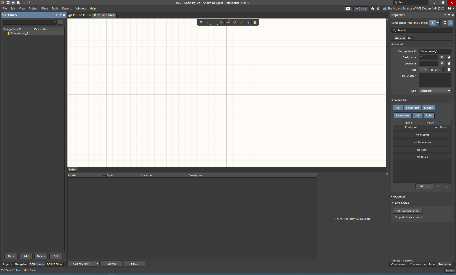
Now we will move on to creating the symbol. As previously done with the PCB Library, add a new Schematic Library to the project.
The schematic library will house the component itself along with its symbol (which we will very soon link to its footprint). Once again, we are provided some tools to create a schematic symbol as well as a few attributes to fill out:
- Design Item ID - The unique name of the component (usually the component’s part number)
- Designator - A general label to use on the schematic to reference this part and others like it (e.g., R1 for a resistor). Since the MIT364-4 is an IC, we should use “U?” where the question mark is an arbitrary number that will be replaced in the schematic.
- Comment - Typically a brief summary of the component, left empty in this case.
- Description - Used to describe the component.
- Links/Parameters/Rules/Models - These are option attributes that can be filled out to provide additional context or simulation models for the component. In this case, we added a link to the MIT364-4’s datasheet.
We now create the symbol for the MIT364-4 (or import a symbol provided by the manufacturer) and add in its attributes. Unlike footprints, symbols are merely a representation of a component for a schematic, so the symbol can take the form of anything as long as it has pins that properly correspond to the footprint. In this case, it will be a box with twenty pins sticking out.
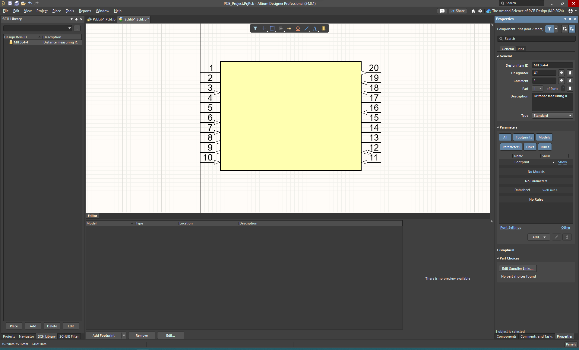
Note that in order for the symbol and footprint to properly mesh together, the pin designators (seen below as the numbers 1-20 associated with each pin) on the symbol must match the name of the pad designators that they correspond to on the footprint. As a quick check, scroll back to the footprint and look to see that there are twenty individually numbered pads that correspond to the twenty pins on the symbol.
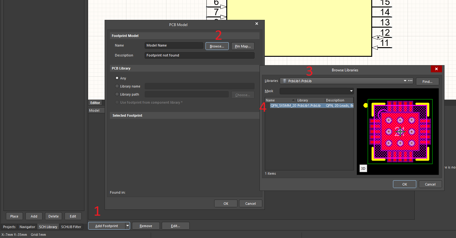
You can now add the symbol by selecting the “Add Symbol” button, which will take you to a dialog where you can search through exisiting PCB libraries (including the one you just made) and select a symbol to link to this component.
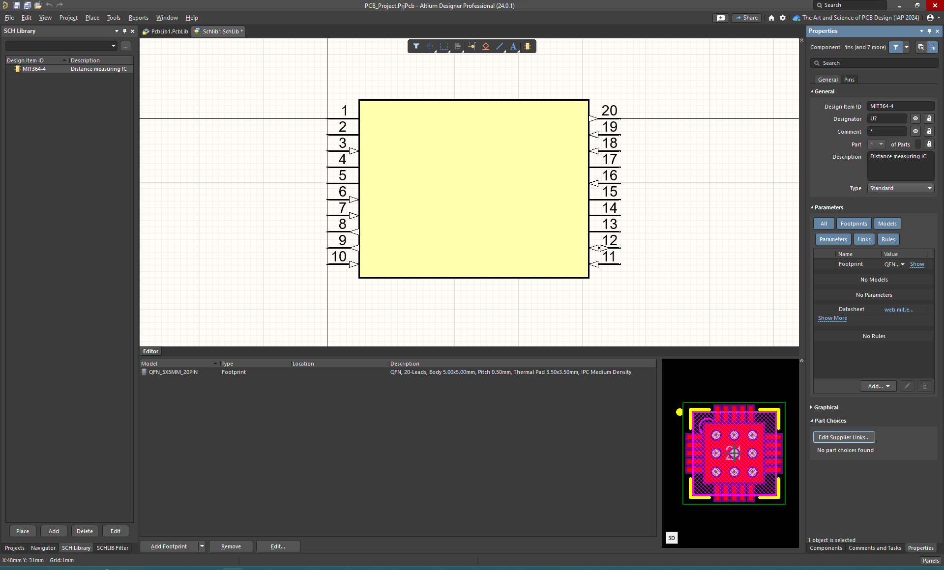
With that, you should see your finished component have both a symbol and a footprint visible within the schematic library. Now you can access this library from your schematic to place the MIT364-4 wherever you please!
References
https://klc.kicad.org/footprint/f2/ https://electrical-information.com/category/electronic-components/ https://workmanship.nasa.gov/lib/insp/2%20books/frameset.html