Suggested Reading
-
Chapter 2 of Designing Electronics that Work covers component selection. We also have an in-depth component selection guide to help you choose components!
-
Chapter 4 of Designing Electronics that Work covers schematic capture. We also have a summary of things to check down below to make sure that we can catch as many mistakes as possible.
Creating the Main sheet
All sheets contains your name and date
Pretty self explanatory. You’d be surprised how many times we forget.
Main sheet contains sub-sheets that are named appropriately
Page 1 of your schematic should be the “main” sheet. This page should contain sub-sheets that mirror the blocks in your block diagram from assignment 1. It’s okay if things are not exactly the same– we understand if you wanted to change some blocks and shuffle stuff. For the main sheet, the expectation is that someone looking at it should understand the general function of your project. This means that sub-sheets should be named appropriately such that their name reflects their function. You can see our example hierarchical sheet here.
Main sheet contains a text box for system description and revision history
Often times, a one-sentence summary of your project can help a lot to explain what the circuit does! A lot of schematic design is not just about making a PCB, but to leave documentation about how a circuit works. This includes revision history, as any future boards you make may go through multiple revisions. It helps to have an easy way to see what revision someone is holding, and to know exactly what’s different between revisions. There’s many ways of revisioning and there’s no standard way of doing it. We’re not going to enforce a specific revisioning pattern since we’re only making one revision; we simply ask that you keep your revision consistent. We’ve been taught one way of doing it however, and you’re free to use it if you choose.
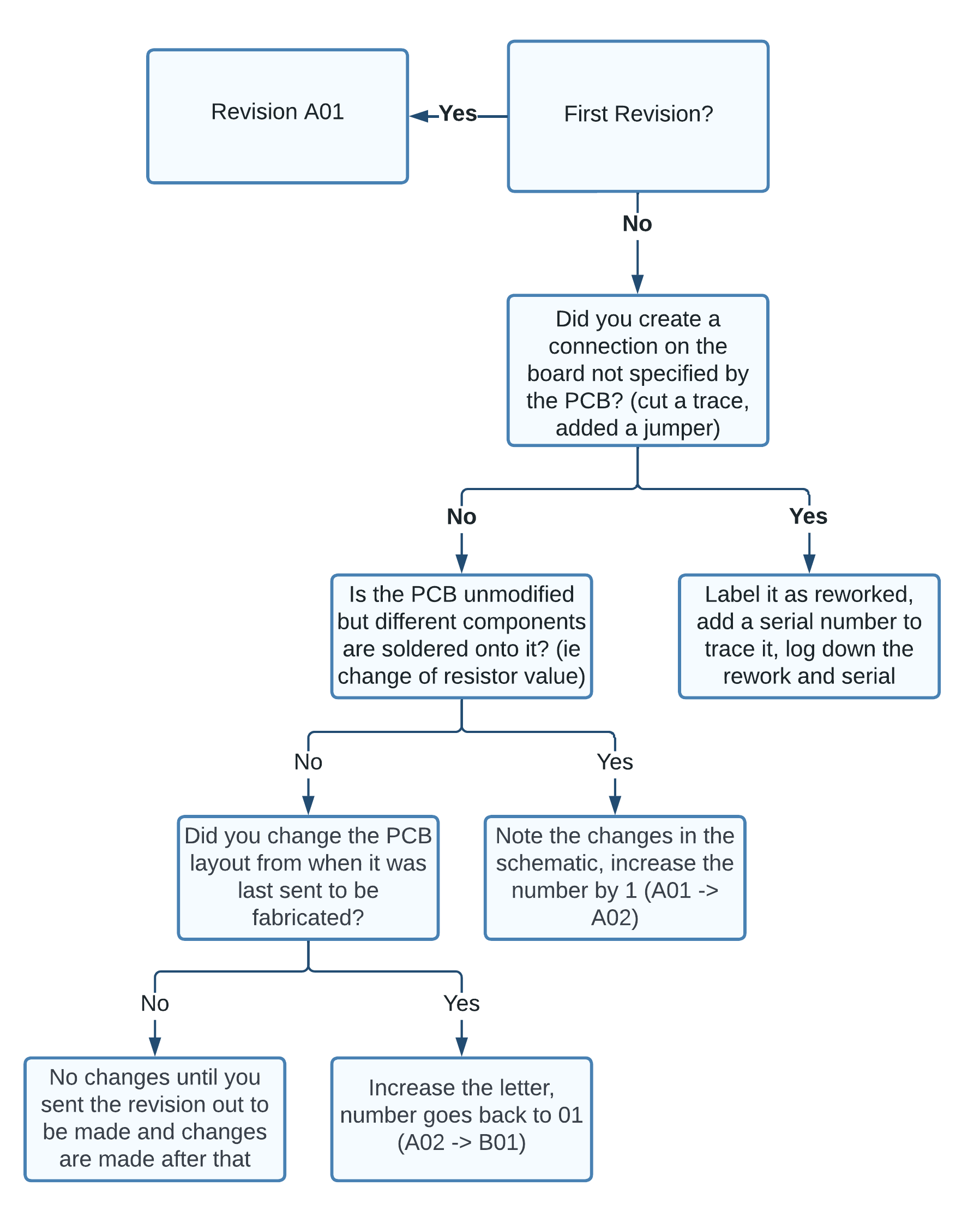
The idea is that the PCB maker and the component assembler (the soldering and testing work) may be different companies. The PCB maker only sees major changes (A, B, C). If a minor change needs to be made, the number can be incremented (A01 -> A02, B02 -> B03), and only the component assembler needs to change their process. The PCB maker can keep making the same board if possible. This helps with avoiding unnecessary lead times, as ramping up PCB production can take a month or more!
[Final Schematic Only] Hierarchical sheets connected together on the main sheet in a thoughtful manner
All your individual circuits need to work together to make one working circuit! Be sure not to forget to connect your circuit together on the main sheet. For the final schematic we expect that you gave your best attempt at ensuring the sub-circuits work with each other. Things like…
- Voltage levels
- Timing
- Necessary pull-ups/pull-downs
Creating Sub-sheets
Short description for each sub-sheet
We suggest that you include a short description for each sub-sheet so the reader will have an understanding of what the circuit does. It helps with readability :)
Important Calculations and specifications listed out
For important values (those that don’t work if the value was 0.1x or 10x the current value), we suggest you list out a calculation or link to suggest why you chose a certain component. This way, if there’s a discrepency when you go to test something, or we want to double check, there’s a good reference.
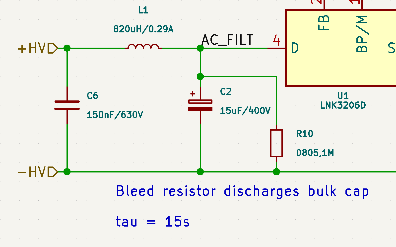
Linking example circuits you used
Often times when looking at circuits, we look at examples to compare and ensure that things match up. Adding a link simply makes that easier.

Passives have proper notation
Resistors
Must specify resistance. Tolerance and package are optional. Default is 0603 Imperial (1206 Metric), 1% for this class. Use the notation
[Resistance Value][Resistor Multipler] (space) [Anything else]
We’re going to be using a Python script to generate order lists for resistors, and this relies on proper resistor notation. If you have special requests, please put them after the resistor specification. For instance, 5.1K 1%, 240R 0.1%. Resistor value should be between 1 and 999.999, and the multipliers are listed below.
| Letter | Multiple | Example | Resistance |
|---|---|---|---|
| m | $10^{-3}$ | 100m | 0.1 $\Omega$ |
| R | $10^{1}$ | 220R | 220 $\Omega$ |
| K | $10^{3}$ | 5.1K | 5100 $\Omega$ |
| M | $10^{6}$ | 3.7M | 3,700,000 $\Omega$ |
Ceramic Capacitors
Must specify capacitance and voltage rating. Package, maximum voltage, and chemistry are optional. Default is 0603 package, X5R or X7R. Popular voltage ratings are 6.3V, 10V, 16V, 25V, 50V. Keep in mind that large capacitors may not have as high of a voltage rated. Naming convention is
[Capacitance] (space) [Voltage Rating] (space) [Anything else]
with no spaces except for those explicitly defined. For instance, 10uF 16V X7R, 4.7uF 6.3V X5R, 100nF 50V. The multipliers are listed below.
| Letter | Multiple | Example |
|---|---|---|
| f | $10^{-15}$ | Too small to use |
| p | $10^{-12}$ | 47pF |
| n | $10^{-9}$ | 100nF |
| u (u as in “you”, not $\mu$ as in “mu”) | $10^{-6}$ | 4.7uF |
| m | $10^{-3}$ | too big to use |
LEDs
Package and color are optional. Default is some 0603 LED we choose semi-randomly.
If you want any special parts that are different from the default specifications, please come talk to us. We understand there are circumstances for their use, but we’d also like to reduce the total number of passives we order. There’s 10 of y’all, and we’re not ordering 10 different 1uF capacitors for everyone to sort through.
All other parts: follow rules for ICs and other active components
[Final Schematic Only] Linking exact parts for ICs and other active components
For most active components, you’ll likely want a specific IC. Be sure to indicate that by ensuring the component name matches with what you want. You’ll also want to ensure that a datasheet is attached to that part to clear up any questions. For passives (Resistors, Capacitors) there’s no need for a datasheet or link unless you need a specific component. Here’s a list of what you should include in the component’s properties:
- Digikey PN (Digikey Part Number)
- MPN (Manufacturer’s Product Name) – copy the exact thing you see on Digikey
For all Sheets
[KiCad only] All symbols must be in one project-specific library
We suggest that at the start, you create one symbol library in the project library table. You can select this in the pop-up after you click create new library in the symbol editor window. Now, with every symbol, it can be imported into the single project-specific library you created and saved in that library. This makes for a much cleaner library than making one library for each symbol.
Thoughtful Net Names
- Inversions are labeled. Example: On the ESP32-S3, the reset line is resetting the ESP32-S3 when it’s low. It’s “inverted” since a “yes reset” is a “reset = 0 / low”. Therefore, it should be labeled as nENA or ENA (in KiCad: type in ~{ENA} for the net label). Both signal an inversion to the logic.
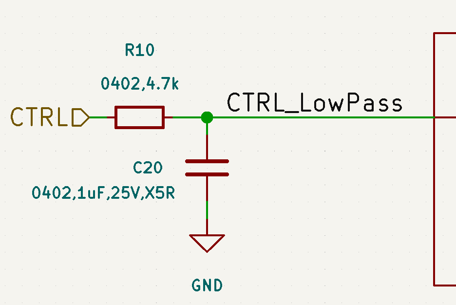
- If going through a filter, label it as [signal] and [signal_Filtered] on either side for read-ability
- If you’re shifting logic levels, label both sides with the voltage. Example: CTRL_3V3, CTRL_5V
[Final Schematic Only] Pin numbers in schematic match those in the datasheet
Let’s look at this LM358 for an example. Depending on the package (the physical manifestation of the thing you put in the schematic), there might be different pinouts! This is why it’s important to check. Let’s say for instance we want to use the LCCC package. The IN1- pin in the schematic should have the number 5, IN1+ should be marked as pin 7, etc.
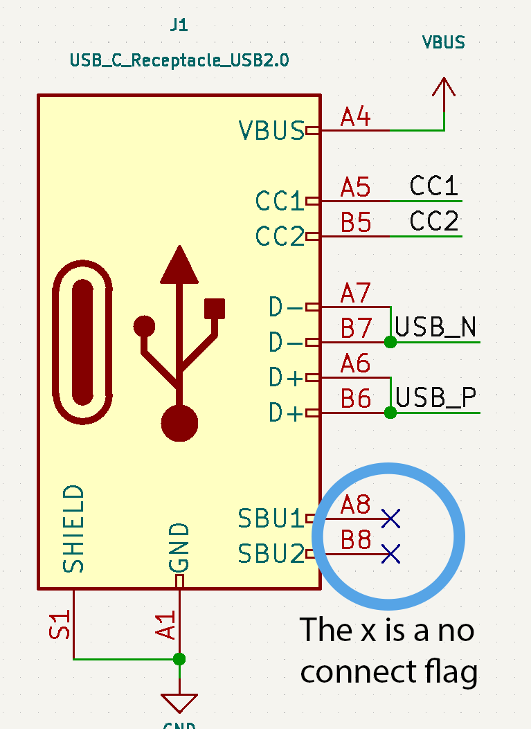
[Final Schematic Only] Unused pins are marked with a no-connect flag
No-connect flags are a good way to tell someone else “I know that’s not meant to be connected” and leaves the ambiguity about why something isn’t connected.
Designators and Names are relatively close to the part
There should be no ambiguity as to which component a designator (The R1/C2/L3/U4/J5 label) and name belongs to. Keep them close to the part.
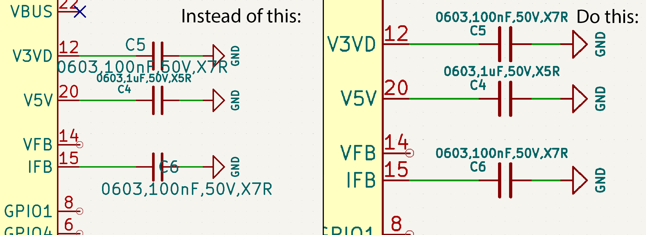
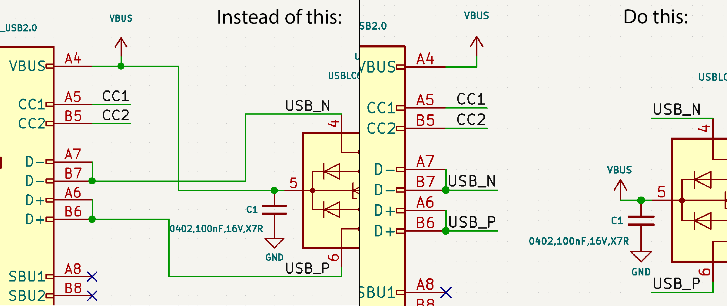
Nets should not be crossing if they’re not connected
It’s extremely difficult to know if two crossing nets are intentionally or unintentionally connected. For this reason, only intentionally connected nets should cross, and there should be no unintentional crossings. This is why net labels are so helpful– they avoid crossing over nets and keep things neat.
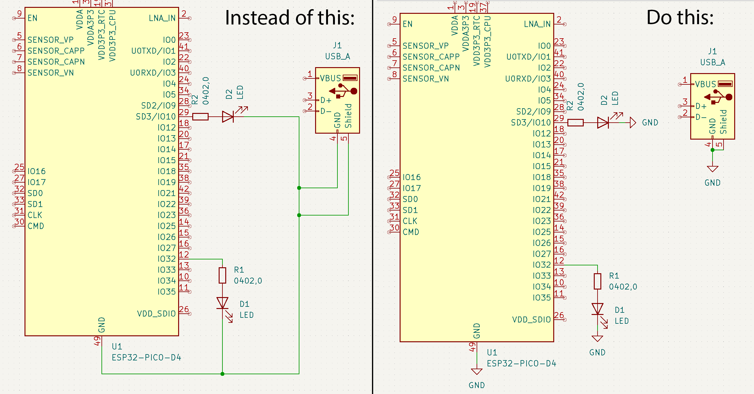
Global power symbols are used instead of nets or net labels
Global symbols are secretly a global net label! You don’t actually need to type out “GND”, the ground symbol does that for you. It makes the ground connections (and other power connections) much more neat and readable.
Turn in your schematic
-
If you’re in Altium, save it and you’re good! We should be able to see it on Altium 365. Please let us know when you’re done by texting in your Slack channel that you finished.
-
If you’re using KiCad, the process will be a bit more complicated. You should have set up Git already. To push your changes into the cloud, here’s what you’ll need to do if you’re using Github desktop:
- Check all the changes you want to save in Github Desktop
- Type a message about what you changed
- Click Commit / Push changes
If you’re using a command-line interface:
- Open a Git command line (might be called Git CMD or Git Bash) window
- Navigate to the main folder of your files. Use ```cd {file name}``` to go to different folders.
- Use ```git status``` to see what changed. You should see ```"Your branch is up to date with 'origin/main' nothing to commit, working tree clean``` if there are no changes, or ```Your branch is up to date with 'origin/main'  Changes not staged for commit:``` if there are changes.
- Use ```git add {file or folder path}``` to add changes you wish to commit
- Use ```git status``` to ensure that the changes are to be committed.
- Use ```git commit -m "{insert your commit message here}"``` to commit your changes. Use a thoughtful message that summarizes the changes you made.
- Repeat doing add, commit until all changes are committed. Often times if a lot of changes are made, you can commit multiple file changes with different commit messages to suggest how each one was changed.
- Run ```git pull``` and make sure nothing weird happens. It may pull from the cloud if you're working with other collaborators, but more likely, you'll get a response of "up to date".
- Run ```git push``` and you should have pushed all your changes!
