Overview
So we have ordered our boards and bought our components, what now?
ASSEMBLY of course! Otherwise known as our board bringup, we need to begin to think about how we will construct our board in a way that best ensures its end functionality. In this lecture we will go over:
- How are PCBs assembled?
- How do we verify that our boards were assembled correctly?
- How do we verify board functionality?
Board Assembly
Reflow soldering
Everyone (at least in this class) has had their moment to hand-solder components. A lot can be done with some wire solder and an iron, and it is one of the most fundemental skills for any electrical engineer to have. So let’s just put our iron to the board and start soldering? Not exactly…
Hand-soldering, while a versatile tool, is not a very efficent process especially for small, mass-produced PCBs. Components are often too small to precisely solder and often (as you likely have seen with QFN and DFN packages), parts have hidden thermal pads that are impossible to reach with any iron. Therefore, we will need a simple, repeatable, and versatile method to assemble our board at scale.
INTRODUCING: Reflow Soldering 🤯
Reflow soldering utilizes solder paste (a sort of liquid form of unmolten solder) and planar application techniques to efficently assemble PCBs with their components.
 Image Credit: StencilMate
Reflow soldering generally follows the process below:
- We take a sheet of metal and make cutouts that matches the shape and size of the surface mount pads on our PCB (our solder stencil)
- We then attach the solder stencil flat with our board and apply solder paste on top
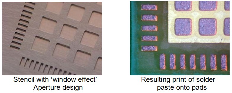 Image Credit: Surface Mount Process
 - With our pads covered with solder paste, components can be placed ontop
- The board is then heated (typically via oven, hot air, or hot plate) to melt the solder and create electrical connections
Reflow is quite a simple process, which also makes it very automatable
Stencils can be quickly laser-cut and attached to pasting machines that can print over multiple boards a minute
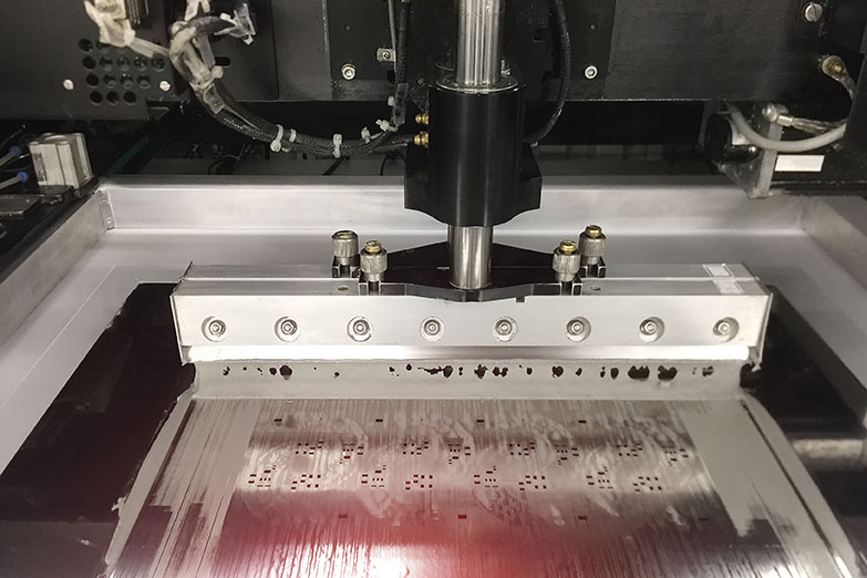 Image Credit: Sierra Circuits
Verification that paste is applied sufficently is also done using specialized scanners
Component pick-and-place machines are used to populate boards with thousands of components a minute.
Specialized reflow ovens can continuously bake boards in an assembly-line
X-ray machines and special cameras can be used to verify sucessful solder connections.
But ultimately what we care about is how can we, as board designers, construct our own boards at a small scale - without the aforementioned equipment?
Stenciling
You will typically find yourself purchasing pre-cut stencils (though with some laser-cutting knowledge, you could make your own!)
Stenciling is all about obtaining the perfect amount of solder paste onto each of your pads. To really show the nuances, let us take ourselves though a typical stenciling process.
The first thing we want to ensure is that we have our board mounted sturdily to our work surface and that our stencil is mounted completely flush over it. Using spare unpopulated boards (of identical thickness to one being stenciled) taped down will help a lot with this
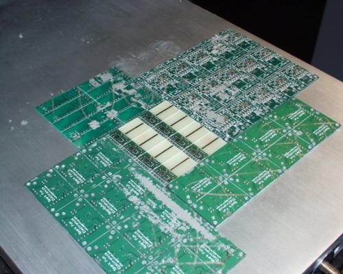 Image Credit: Sparkfun
With our board secured in place, we can align the stencil on top and tape it down too.
Afterwards, we will put down a generous line of solder paste on one side and use a credit card to squeegee the paste from side of the stencil to the other all in one go. For large designs, it may be necessary to do multiple overlapping swipes to cover all pads
Below is an example video guide showing these steps in action (from IAP 2023).
Once the stencil is removed, we will want to make sure everything has been pasted correctly, and a quick visual check will suffice. Component pads should nearly be completely covered in solder paste in an even manner consistent with the shape of the pad/stencil.
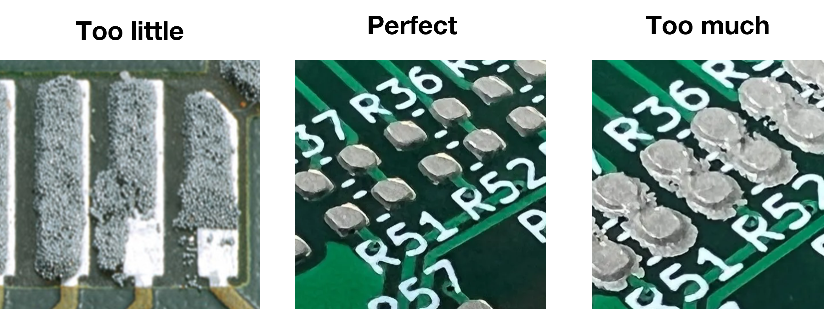 Image Credit: Sierra Circuits and Leeman Geophysical
If a re-stenciling is required, solder paste can be easily cleaned off with a wipe and rubbing alcohol before it is reflowed.
Component Placement
This step is pretty self-explanatory. You will want to take your components and placed them on top of your board such that they rest on top of their respective paste-covered pads. At this point the importance of component orientation markers and reference designators to aid with assembly become quite clear.
Placement can often be more forgiving than you think. During reflow, when the solder paste melts, surface tention will tend to bring the component’s leads in line with its pads. So if a component is mis-aligned by a degree, do not worry too much about realigning it.
Reflow
Reflow can be done a few ways
- Hot plate: boards are placed a flat on a hot plate and heated until the solder liquifies
- Very simple process and easy to track visually
- Important for the hot plate to provide a relatively even heating surface; wide temperature differences in a board can cause warping. Heating the board on top of a bed of sand is one way an even heating surface can be provided
- Works only with surface mount components; through-hole parts make it impossible for the board to lie flat
- Hot air: a very hot air gun is used to reflow components individually
- Great for precise reflow where one does not want the entire board to be heated at once.
- Time consuming process and often requires the board to be preheated under a hot plate to prevent warping
- Use a low air speed or components can go flying
- Caution around plastic components, excessive heat can melt them
- Oven: boards are placed in a reflow-specific oven which heats up the boards in a pre-defined pattern
- Best for high-production needs and can lead to the most consistent results
- Requires specialized ovens that can follow solder reflow curves
- Caution around plastic components, excessive heat can melt them
All solder pastes come with a recommended reflow profile which defines how long and at what temperatures a board should be heated in an oven in order to maximize reflow success and avoid damage to the board and its components.
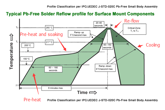 Image Credit: Bittele
Once we have finished reflowing our board, we will need to visually inspect it to ensure all the paste has melted and is properly binding each component lead to its respective pad. For most components, this will be pretty obvious. We want to see silvery fillets along each pad and pin.
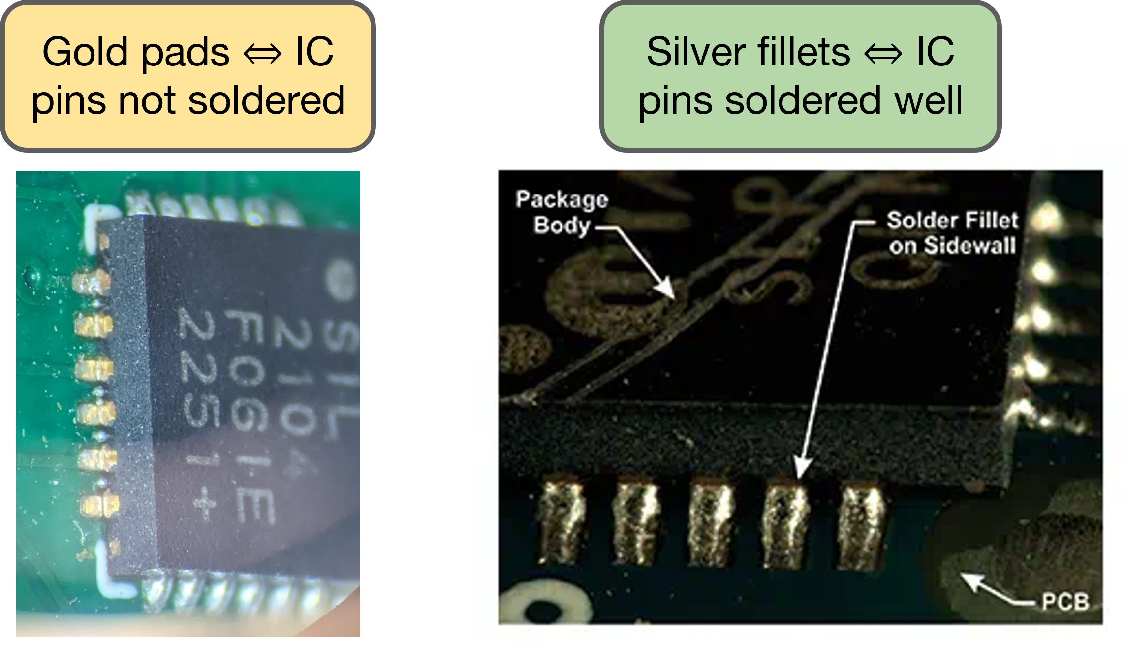
Pins/pads that fail to meet this standard may not correctly conduct, you will need to manually adjust them using additionally reflow (i.e., hot air) or with some precise soldering iron action.
Bringup
Reflow is an inherently volatile process and it is for unnoticed mistakes to creep in that affect board functionality, especially for newly designed PCBs.
To address this problem, we use bringup plans outline an piecewise assembly procedure that eases testing and debugging.
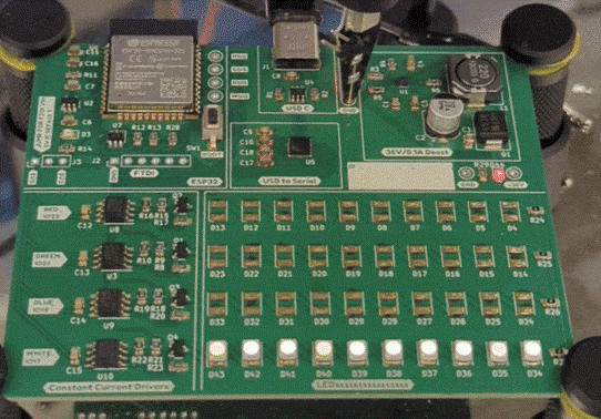
Let us use the LED demo board as an example. Bringup relies heavily on our system block diagram:
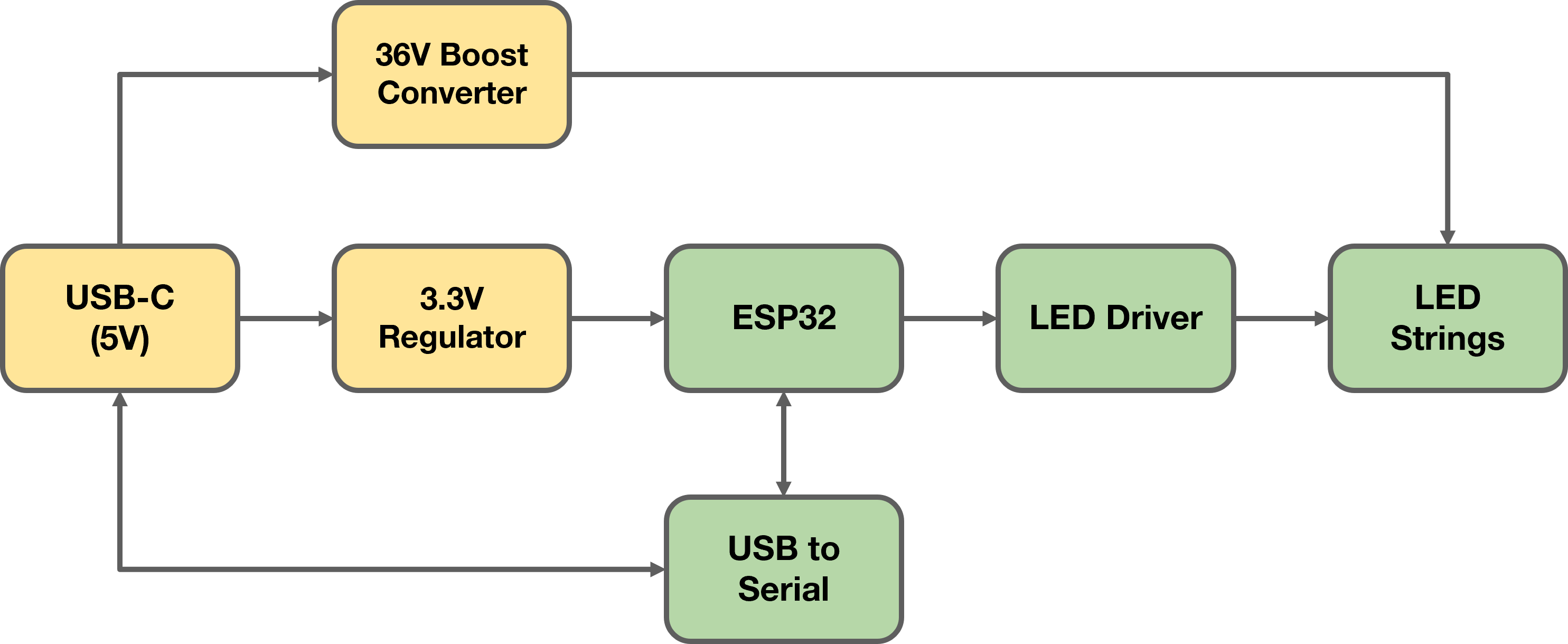
Start off with the sections that are relied on the most, and often that will be the power supply/distribution.
We want to ensure the system fails “safely” if anything goes wrong, particularly when it comes to the power supply. If a section work incorrectly, we do not want it to cause damage to other sections, in addition to itself. Achieving this can be done in many ways:
- Populating sections one at a time
- It is impossible for improperly functioning components to damage components that are not even placed on the board. Doing this in a well-planned, serial fashion can really help to isolate bugs and issues with the board. However, it can be quite difficult and tedious to assemble, especially with reflow soldering.
- Utilize jumpers and zero-ohm resistors
- Hopefully during schematic, you used a plentiful number of zero-ohm resistors as jumpers to isolate sections and components and make testing easier. Waiting populate these after testing can help in discovering issues while protecting components, and is makes solder reflow much easier
- Conduct incremental tests
- Using external power supplies, we can apply power to specific circuits and sections in a controlled manner to test functionality while preventing a damaging fault. Utilize the over-current features of your power supply wisely.
For our LED demo board, we can choose not to populate the zero-ohm resistors connecting our 36V power supply to our LED strings, which allows us to test the power supply without damaging the LEDs.
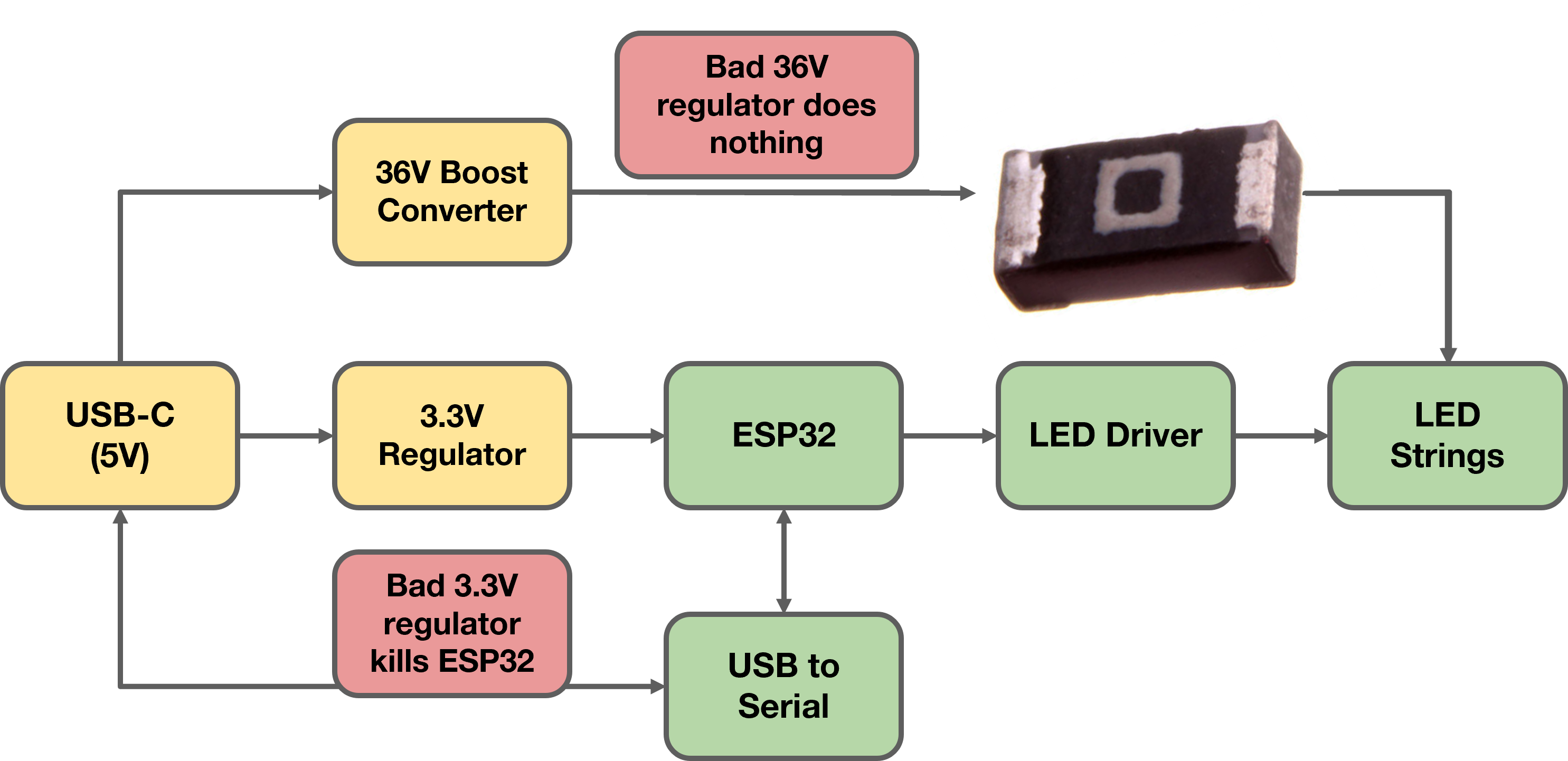
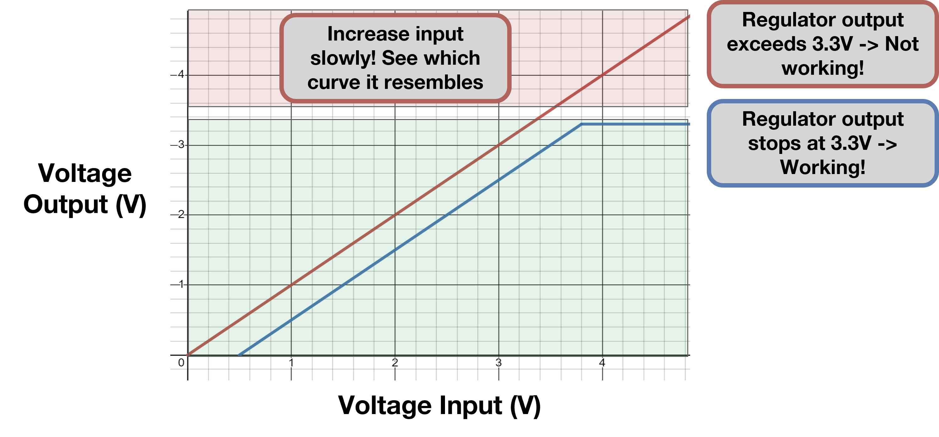
But what about our 3.3V regulator! No jumpers? No problem. We can still validate its functionality safely without having to isolate it from the rest of the circuit. By gradually increasing the input voltage into the regulator, we can check that it keeps the its output at or below 3.3V, even when we increase the input beyond 3.3V. Do this slowly so that if the regulator does not work, downstream components only experience a slight overvoltage if the regulator does not end up working, which they can handle.
Finally, we will test the microcontroller, which we can do by running test codes to demonstrate functionality.