Overview
Debugging is really only necessary because we are never perfectly certain what is going to happen with our PCB. Simulations and models can help us predict, but nothing can replace real-world operation. This is especially the case when dealing with real components. As discussed in lecture 02 our “100H inductor” might not be exactly 100H, it might saturate differently than the datasheet says it does, or contain parasitic elements that limit its high-speed performance.
However, what is more likely the case is that we might just forget to model something in design, or we fail to realize we need to(engineering is a science after all). These errors can cause issues in our boards that we can fail to forsee.
Through the process of debugging, we utilize our knowledge of our design and how it should function to identify and fix issues caused in manufacturing or in our design. This is why understanding how your own circuits fundementally operate is so important in PCB design.
On the brightside, debugging often consists of identifying very common errors and can be done with common tools.
Tools for Debugging
Multimeters
Multimeters are the first tool we can utilize when we encounter a problem with a circuit. They can give you incredible amounts of information very quickly and help you rule out possible issues fast. Here are a few types of checks multimeters can run.
Voltage
Voltage measurements involve checking the potential difference between points in a circuit and are a super useful test. You simply place the red probe on one point on the circuit and place the black probe on another.
Continuity/ Resistance/ Diode Checks
Continuity tests are honestly one of the most useful checks while debugging. We use them to most just to sanity check that all parts of the circuit are connected and that different nets are not shorted together. Sometimes when one pin of a QFN does not reflow properly, or you need to check if a switch, relay, or MOSFET is turning on and off correctly, a continuity check can be super useful.
Current
Current tests are not as useful as a debugging tool but important when characterizing systems. Use caution with these measurements as most multimeters can only measure up to 10A before they explode. Improper current measurements can also lead to inadvertent short circuiting.
Oscilloscopes
Oscilloscopes are an incredibly powerful tool for debugging. They can capture extremely fast analog or digital signals with high resolution. We use them very often in debugging because often we have an understanding of what the signal SHOULD look like but we need to check if the circuit is actually producing that waveform. If you are just checking a signal that is supposed to be an unchanging DC voltage, generally you would want to use a multimeter. But if you want to see a sine wave, a pwm signal, or something more complicated - like the input and output of a filter - you want to use a scope.
Logic Analyzers
Logic analyzers, like oscilloscopes, measure signals that change in time. However, logic analyzers can only measure discrete signals that change between an OFF and an ON state. They are perfect for debugging communication systems and other digital signals because they come with processing logic to translate measured ON-OFF signals into readable data. Logic Analyzers can be used on communication systems like I2C, SPI, and UART to read and decode signals. You can actually see the values of the bits being sent over the wires using a logic analyzer.
Power Supplies
Now you may not initially think of a power supply as a debugging tool, but it is more useful than you might think. Often times when we are getting bad signals in a circuit, or if parts aren’t turning on, it is useful to be able to inject voltages into a circuit to test components or to make sure the correct voltage is being supplied. For example, if a circuit runs on a battery and you are unsure of the battery’s voltage, or if you’re reading from an analog sensor and you are afraid the output might be wrong, you can test the circuit by injecting a correct, known voltage to determine if the battery or the sensor is faulty.
The MIT Solar Car Battery Characterization Document shows the use of a power supply to fake a current signal to test a Battery Management System.
MIT Solar Car Battery Characterization Document
Strategies for Effective Debugging
Note that there is no set law for how one should debug, but we can utilize different strategies to best increase our chances of identifying issues and fixing problems. Good debugging requires an understanding of the laws of physics and how circuits work - sometimes even down to the component level. The more time you spend debugging circuits the better you get both at debugging and design. The best design principals for electrical systems are usually extracted from debugging boards. Everytime someone tells you “you should do this,” in electrical design. Try to imagine the situation that caused someone to realize that and reason it out.
Here are a couple of debugging tips to apply when something “isn’t working.”
- Check continuity: turn off the board, and make sure the things you expect to be connected to each other are connected. For example, let us say we notice a communication signal is not being sent/received or a component is not getting power. Probe from the LEG of a chip (say the transmitter or power regulator) to the LEG of the other chip (the receiver or component needing-to-be-powered), and NOT from pad to pad. Testing the continuity from one pad to another pad will help determine if a trace is broken, but will not rule out if a solder joint is improper, which is often the case. A lot of issues come just from bad solder joints.
- Check voltages: make sure everything is getting power (and the right amount of it) and make sure that signals are are outputted at the magnitude and frequency that is expected.
- For precise signal measurements, you can break out tools such as a oscilloscope or a logic analzer, and use these to probe signals to make sure they are what you expect them to be.
DEBUGGING IS PURELY ABOUT PROBING. PROBE PROBE PROBE YOUR CIRCUIT. Each time you probe something you learn something, even if you think something is fine, probe it. It’s one less thing to worry about. The greatest barrier in debugging is remembering to pick up the multimeter. Just make sure it’s on the correct mode XD.
Case Study
Let us use our LED Demo board as an example for debugging. It helps (perhaps only in this case) that there were a few errors in the board from both manufacturing and inherent to its design.
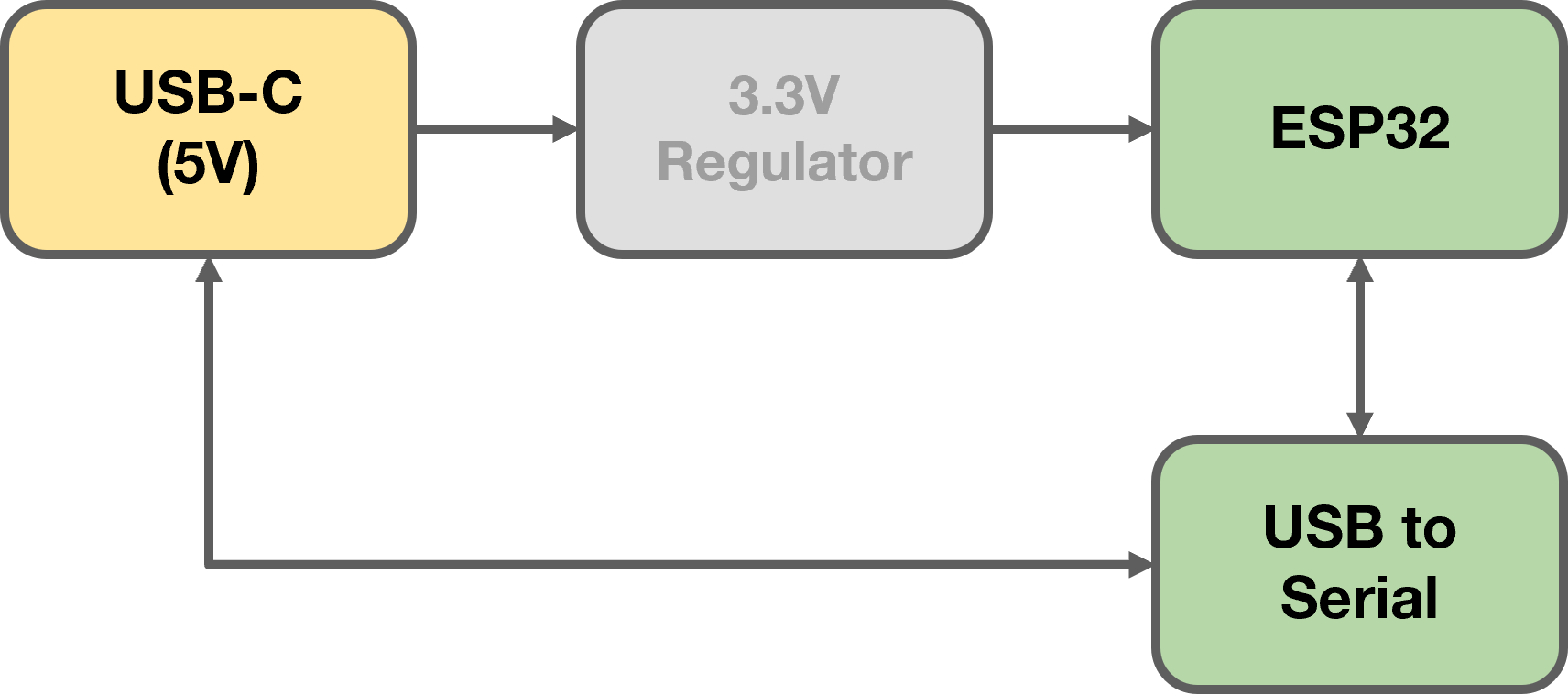
Recall again the system diagram:
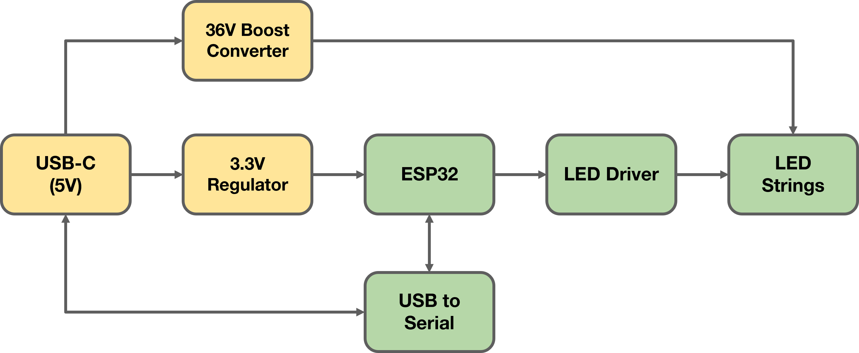
There is a lot that could go wrong with a board of this complexity.
Soldering
Bad solder joints are easy to make with small components with even smaller footprints. Some components are also affected greater by bad solder joints and improper connections. For the LED board in particular, the 36V boost converter, ESP32, and USB to Serial blocks are affected the most by bad solder connections because of the packages used by their ICs.

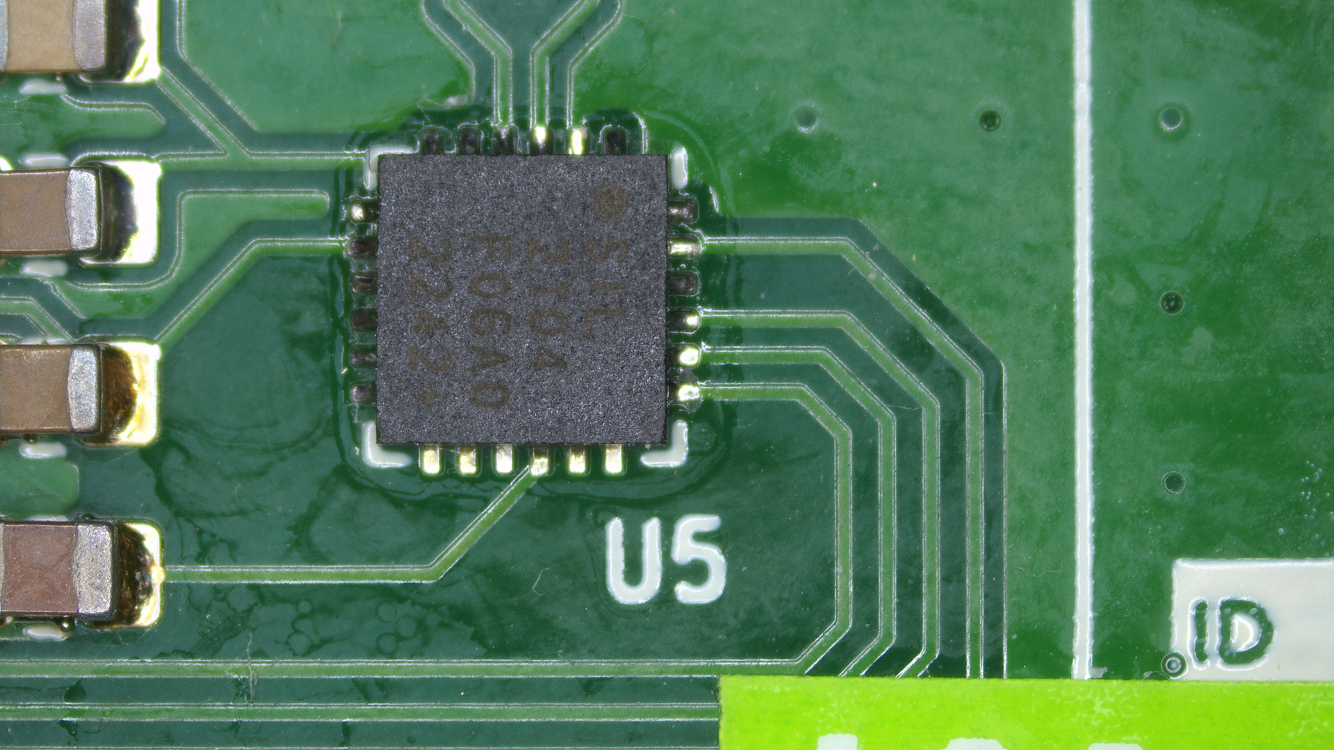
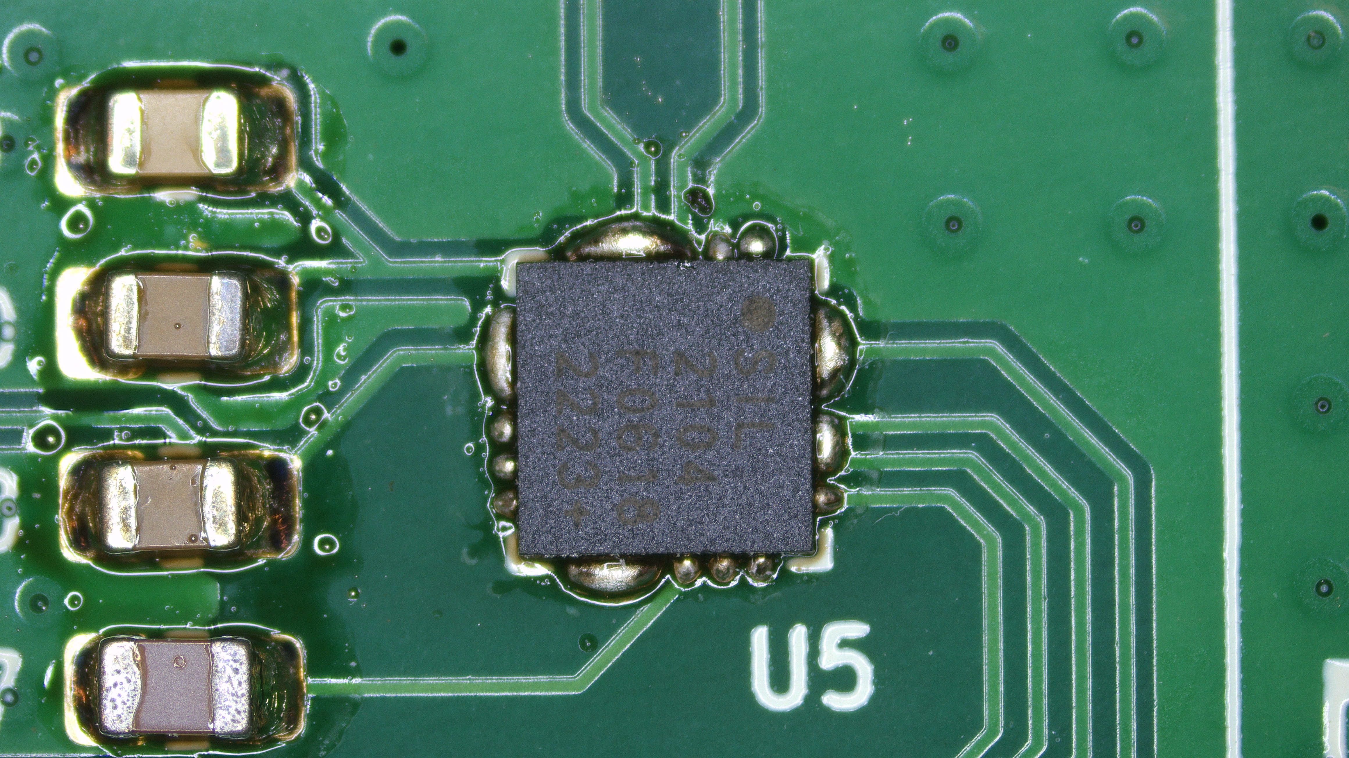
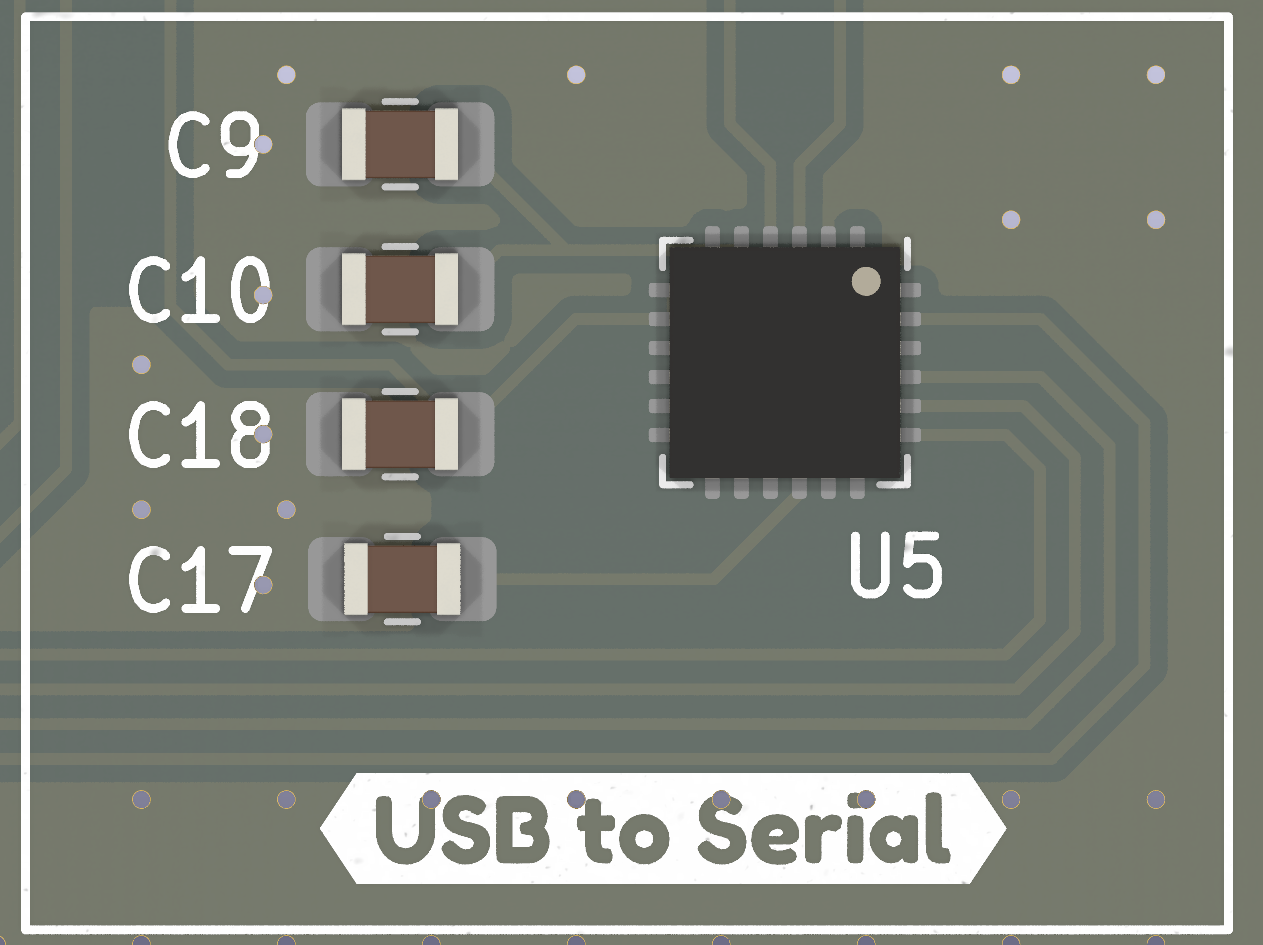
A visual inspection can be incredibly useful to determine whether or not proper solder connections are present. As mentioned in lecture 06, small components will often have gold plated pins, which should become completely silver and covered with a fillet after reflow soldering. In the USB to Serial chip below, notice how the bottom row of pins lacks enough solder (from its flat gold color) while the rest have been reflowed perfectly.
Be sure to also check for too much solder! They can easily lead to shorts between pins.
And the same applies for the boost converter IC.
Removing excess solder from small components like those above is as simple as using a clean soldering iron (use a brass sponge on it until the tip is silver-y) to quickly melt the solder beads. Surface tention will cause some of the solder to melt onto the clean soldering iron tip and remove itself from the pad. When this happens, remove the soldering iron, clean it again, and repeat until all the excess solder is gone.
For large pads with a lot of excess solder, or to desolder a large component, solder wick can be used. Solder wick is made of a flat braid of copper wires soaked in flux. When sandwiched between a pad full of solder and a hot soldering iron, the solder melts and flows into the braid, which wicks the solder away from the pad.
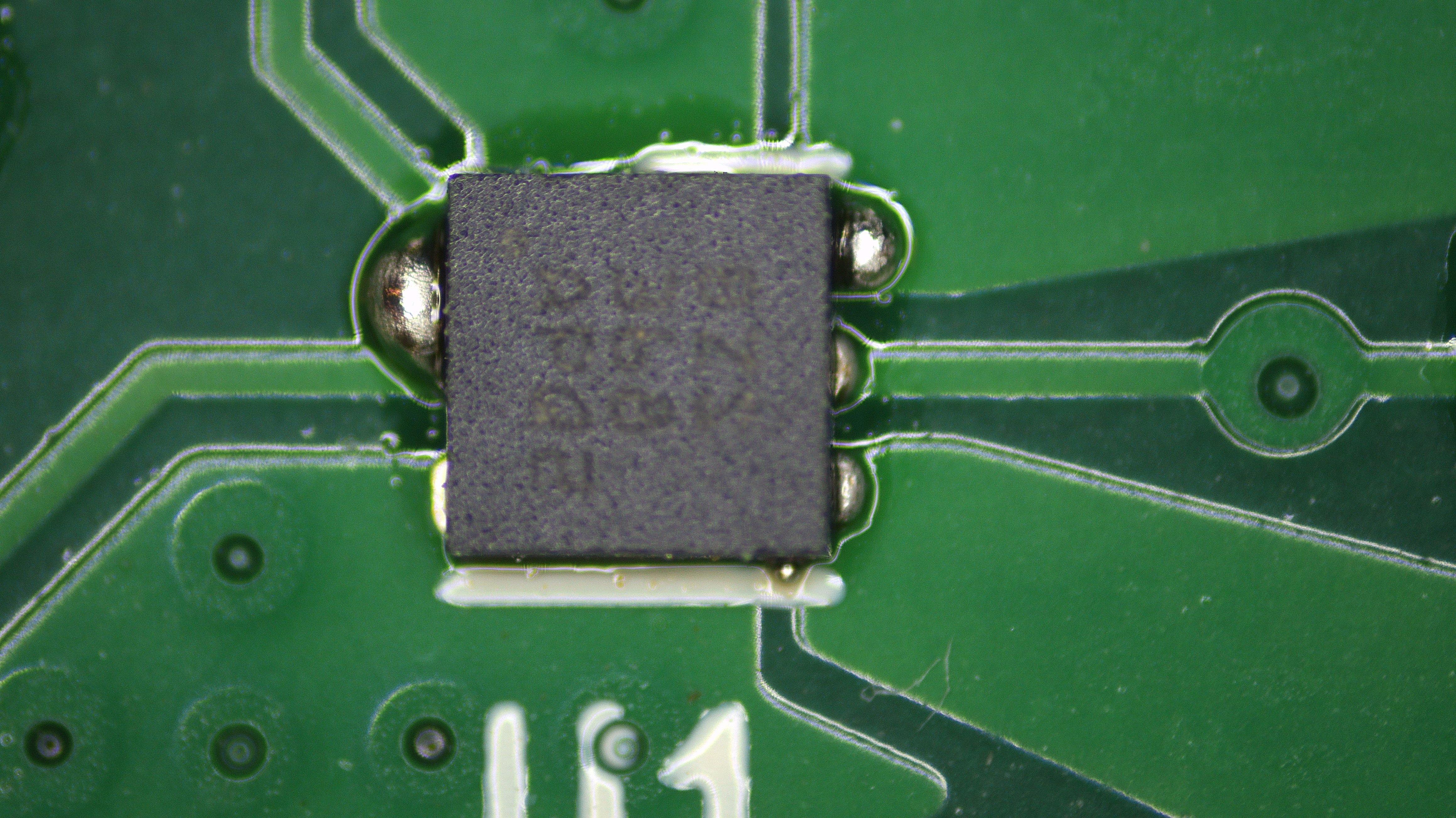
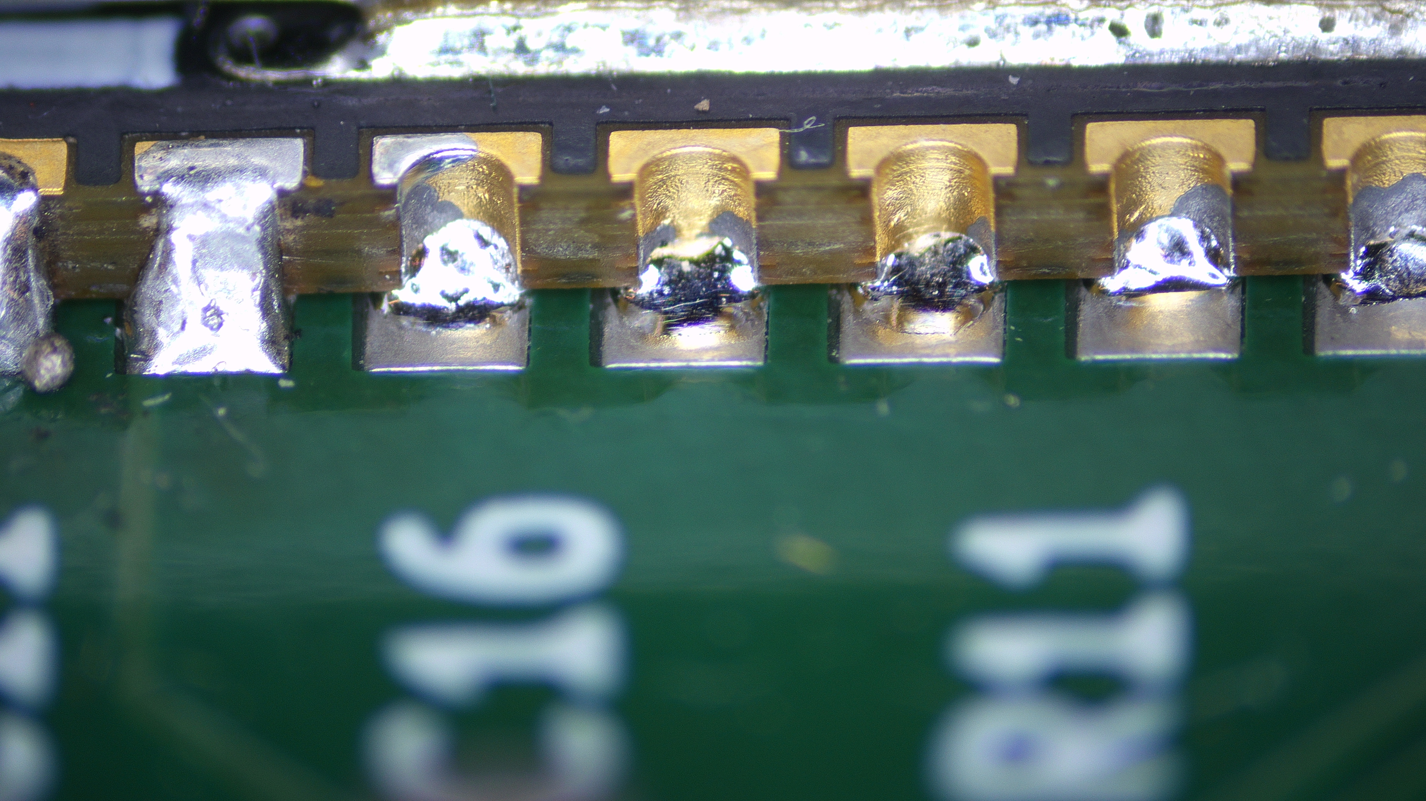
Large castellated pads, like the ones on the ESP32, may require more attention then one realizes. Often reflow may not heat the pads enough to coat the pad fully in solder. Be sure to check these castellated pads and add solder by hand as appropriate. In the photo below, only the leftmost pad contains an adequate amount of solder and has created a strong electrical connection. The rest of the pads will require additional rework.
Incorrect components
Often due to sourcing issues or by mistakes in procurement, incorrect components can find their way on to our board. In our case, the resistor R4 is part of the feedback network for the 36V boost converter circuit. Put simply, R4 helps determine what the output voltage should be.
Calculations tell us that R4 should be 10.1 kOhms to have the boost converter output 36 V. However, perhaps upon a second look by a reviewer who does not fully understand the circuit or by those in component procurement looking to order only common components, R4 was rounded down to 10 kOhms. This is a common practice and for many circuits this can be completely fine. However in the case of our boost converter, it leads to the output being 38 V, which could potentially ruin the rest of our circuits!
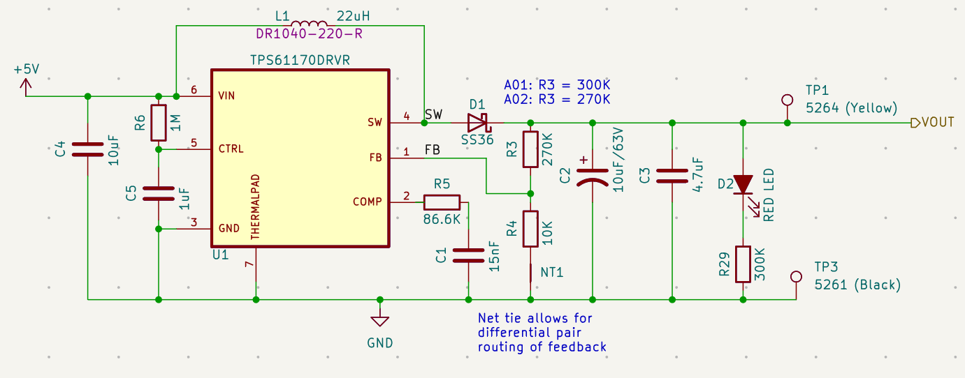
A methodical bringug plans and circuit tests are important to identify defects such as this (recall lecture 06). For this kind of error, the solution is as simple as replacing the part with a resistor of the correct value. Thank goodness!
Incorrectly placed parts
Except for passive devices, most components are going to have some sort of polarity or orientation direction. Some parts (like USB connectors and ICs with asymmetric packages) are pretty easy to orient and will often have footprints that make incorrect mounting a feat of engineering and thought. Unfortunately, lots of other device do not - and as is the case with many square-shaped ICs incorrect orientation is possible in three different ways!
Such is why orientation markers are crucial during the design process to aide the board assembler (often ourselves) with constructing our PCBs in the correct manner. Therefore, in the absence of markers, it can often be one of the more common issues causing board malfunction. It is a good idea during the debugging process to visually verify that components are placed correctly (your PCB layout software can help a lot with this) and to make the obvious check that the correct components are in the correct places too, as devices can share footprints.
With our LED demo board, an easy mistake to make is to mount LEDs backwards or the USB to Serial IC in the wrong orientation. IC markers can be quite small and silkscreen orientation markers obscured by solder paste or destroyed during fabrication.
Signal timings
With more complicated systems that involve fast communication between devices, signal timings can become very crucial to proper circuit operation. We can often probe and ensure these specifications are met by using an oscilloscope or logic analyzer.
Signal timing issues often occur in traces that have been incorrectly routed (too long or too short), within transient RC circuits, or in filter networks.
Our LED board contains two circuits with strict timing requirements:
- The ESP32’s reset/boot mechanism
- The USB data differential pair
The ESP32 relies on its boot pin be pulled high before its reset pin in order to enter in download mode (to receive programming data). On the LED board, these two pins are electrically connected together during programming, so to enforce the delay between the two, an RC circuit is employed on the reset pin to slow down its signalling. Incorrect values for the RC circuit can prevent the correct delay from being reached and prevent the ESP32 from entering its download state. Using an oscilloscope in its event-trigger mode, probed on both the reset and boot pins can help catch errors like this.
As was mentioned before, the USB data lines are defined as differential pairs (having a 180 degree phase shift relative to one another). Incorrectly routed traces (where one trace in the differential pair is longer/shorter than the other) can result in the loss of this phase relationship. Probing using a triggered oscilliscope can help identify whether or not these signals remain at a 180 degree phase shift of another.
Fixing Errors
We finished debugging and found every problem with our circuit, now how do we fix them?
Ultimately, the problem defines the fix but below are some techniques for performing particular PCB repairs:
- Component replacement: an incorrect or faulty component can always be desoldered and a correct/new one soldered in its place
- Fixing bad solder joints: there are many ways to do this.
- Single solder joint mistakes can often be fixed by hand with a soldering iron, extra solder, flux, and solder wick
- For chronically bad solder joints throughout a board (often caused by bad reflow), a board can be re-reflowed to re-melt paste and hopefully fix many of the solder joints. This method should primarily be used for boards with bad initial reflow (such as insufficiently melted solder paste) as each addition reflow attempt can damage the board and its components
- Adjusting nets: traces on outer layers can be cut using a sharp knife to sever nets and thin magnet wire can be used to form new nets
- Soldermask can be scraped off traces to reveal the copper underneath to solder new connections/wires
- Often there is extra space on pads to solder wires
- Careful population or desoldering of components can free up pads to help build new nets.
- Having test points connecting to important nets makes fixes much easie
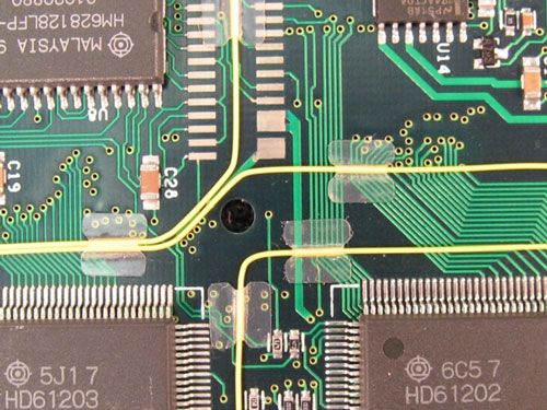 Image Credit: CircuitMedic