00 – Nonlinearities and Nonidealities
One of the big jumps when going from a schematic to a real system is the non-idealities in all the components that are used. Ideally we’d like our capacitors to be capacitors, our inductors to be inductors, and our resistors to be resistors. The real world is unfortunately not like this. These are all things we need to keep in mind. We need to know what to look for in datasheets so our systems can be designed to work not just on paper, but in real hardware. This lecture will explore this.
01 - Parasitics in components
A parasitic is something that we don’t want. Often times, parasitics are something that we can’t eliminate because of certain manufacturing processes. They’re like engineering tradeoffs– different components will have different parasitics, and it’s up to us to decide which parasitics we’re okay with to maximize our performance without paying more for quality we don’t need.
01.01 - Capacitors
Let’s first look at capacitors. One parasitic that might be more apparent is an equivalent series resistance, or ESR. We’re doing to define the ESR as a resistor in series with the capacitor under test. In the most extreme case, the material that the capacitor is made of must have some resistance. This resistance means that even if the impedance of the capacitor is very low, the resistance sets a minimum impedance that the real capacitor can be. In addition, the geometry of capacitors can cause to have inductive effects. This means at very high frequencies, the capacitor actually acts as an inductor, not as a capacitor. For this reason, be careful about what capacitor you choose, and make sure it actually acts as a capacitor in the frequency range it operates at. Below is a typical plot of the capacitor impedance over frequency.
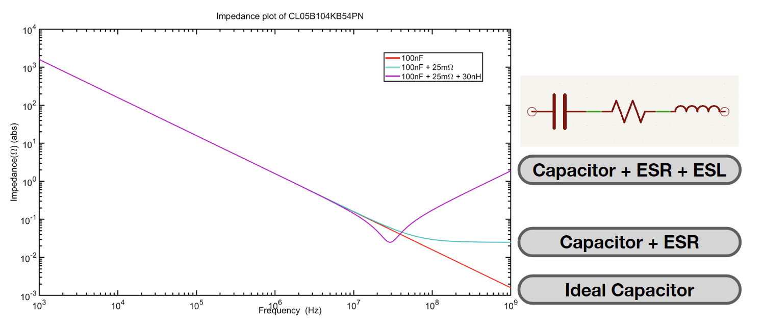 Various capacitor models vs frequency
Different capacitor chemistries also result in different volumetric capacitance density. Electrolytics tend to have the highest density, while ceramics have a lower density, and film capacitors have the lowest density. Let’s talk about when we’d use each chemistry.
Electrolytic Capacitors
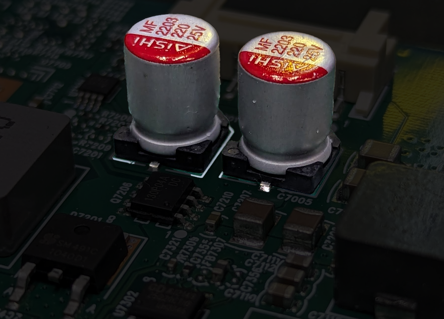 Photo and editing credit: Winnie Szeto
The large volumetric energy storage in electrolytic capacitors makes them ideal for use as bulk capacitors. This is when the capacitors are used as a quick and low-impedance energy source. It’s like your cupboard. It’s fairly easy to get food from your cupboard, and it’s much more convenient than getting it from the store. It may not have the variety of food as a supermarket, but it holds a fair amount of food, meaning that you shouldn’t need to go to the store every time you’re full. With the bulk capacitor, it’s quite similiar. Let’s say a power-hungry device like a motor wants to quickly turn on. If it tries to get power from the power source like the power supply or a battery, they’re far away and have lots of resistive and inductive parasitics. Instead, there’s a lot of energy stored in the bulk capacitors on the PCB! These capacitors store enough energy to supply the motor with quick bursts of energy. Slowly, the larger power source will recharge the capacitor as its charge begins to drain. This prevents the voltage from suddenly dropping if a load was pulled. Notably, bulk capacitance is used for an entire system’s energy storage. For instance, one may put a lot of capacitors near where the power entry happens. The capacitors pictured above are 2x 220uF 25V Solid capacitors. They’re both placed next to the power entry connector, allowing for a cleaner 20V DC power entry into this display controller board.
Ceramic Capacitors
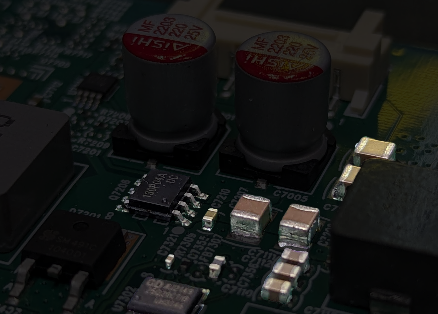 Photo and editing credit: Winnie Szeto
When it comes to ICs (integrated circuits, the black boxes with legs), they need a similar system of power delivery so they don’t shut off. Typically ICs draw significantly less power than large power hungry motors, so they won’t need the big electrolytic capacitors. Rather, they need less but much faster bursts of current. This is where multilayer ceramic capacitors (MLCCs) come in. Their low ESR/ESL means their operating range is in the MHz range, making them great for fast switching ICs. The lower energy storage isn’t as big of a deal, as the current draw is probably multiple times lower than what a bulk capacitor might expect. This type of capacitor usage is called a bypass capacitor, as it ensures the little ripples in the supply voltage don’t propagate to the IC. Bypass capacitors are often placed close to the IC that’s being bypassed since that reduces the ESR/ESL losses that may reduce the operating frequency fo the capacitor. This means that bypass capacitors are used near every single IC. Think of these like the snack pile next to your desk. Not as much storage as the larger pantry [Electrolytic capacitor], but probably stores enough for the fast spikes in snack cravings [current]. You can see that in the image. The ICs (black boxes with legs) have smaller bypass capacitors (the smaller orange colored boxes) next to them, likely where the IC has its +V pins. If you’d like more information on selecting capacitors, check out our Component Selection Guide.
01.02 Inductors
01.03 Resistors
01.04 Silicon
02 - Practical Circuit Design
Now that we’ve looked at individual components, let’s zoom out and look at circuits– how they interact with each other, and what things we need to consider when designing a system.
02.01 - Pull-ups and Pull-downs
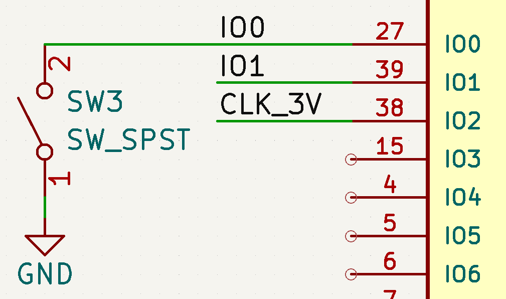
Let’s suppose we’re using SW3 as a button input for our microcontroller to read on the IO0 pin. We know that when the button is pressed, the switch connects IO0 to ground and IO0 is now low. But what about when the button is not pressed? When the switch is open, there’s nothing connected to IO0, so there’s no way to reliably determine its state. We’d like it to be high so the pressed and not pressed state are different to the microcontroller reading the state.To do this, we can add a resistor in the $k\Omega$ range from IO0 to +3.3V.
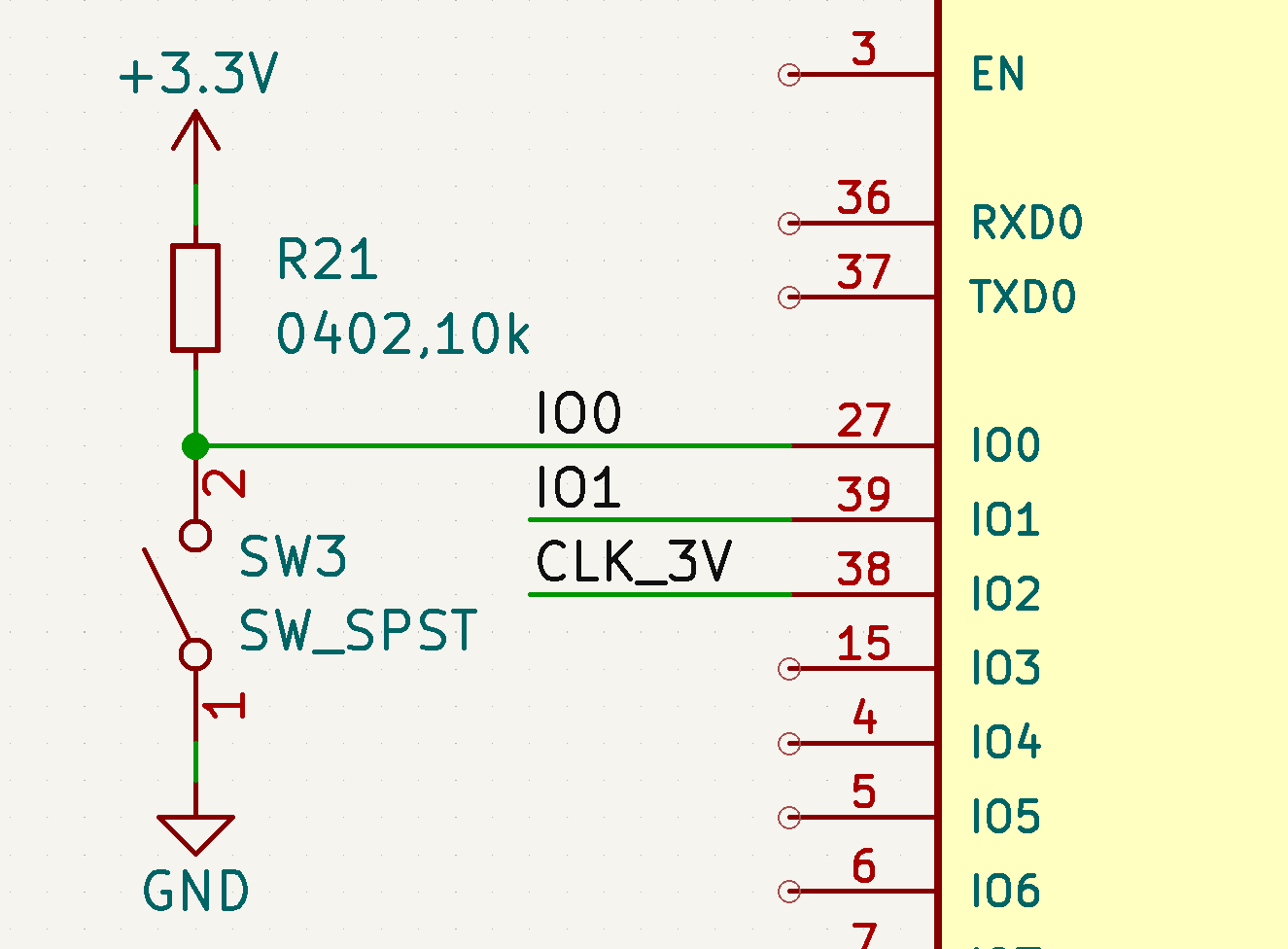
With this resistor, IO0 is high when the switch is not closed since the resistor pulls up the IO pin to 3.3V. For this reason, the resistor is called a pull-up resistor. When the switch is closed, it makes a resistor divider with a $0\Omega$ resistor on the bottom and a $10k\Omega$ resistor on the top. This means the closed switch still results in IO0 being low. Great! We’ve solved this problem and pull-ups ensure that we can always define a signal. Pull-downs (to GND) are used in the same way if we want the not active state to be low.
02.02 - Delay Circuits
Sometimes you’ll want to turn on circuits after a certain time delay. Perhaps you don’t want every single IC turning on right when you plug in a device. Sometimes you can trip overcurrent protection if everything turns on at the same time. Other times, your circuit might want a specific thing on first. For instance, if we wanted to power on the microcontroller before the lights got power. Let’s explore how we can delay the +36V rail’s power up to better control how our device turns on.
Reading the datasheet, the TPS61170 specifies that a 1.2V signal on the enable pin will result in the IC turning on. By default the enable signal is hooked up to VIN, so the IC turns on right when power is applied. If we want to delay this chip from turning on immediately, we’ll need something to keep the enable signal low for a set period of time. If we can utilize a passive solution (ie something that uses an analog filter) then we don’t need a complicated discrete solution(one with more ICs and timers)!
You might recall a low-pass filter’s step response delays when the voltage rises. We could use something similar here! Let’s say we want a time delay of around 300ms. We could use a 300K/1uF low-pass filter as a start, since that has a time constant of 300K * 1 uF = 0.3s. One thing to look for is this IC actually has a built-in pull down resistor of 800K on the enable line. We’re going to want to include that resistance in our model. THe easiest way to analyze this circuit is to use a simulator. We’re using CircuitLab as it has a free license for @mit.edu emails. There’s various other tools, and your ECAD software might even have some built in! We just like CircuitLab since it’s easy to use. The 300k turns out to be too low, so it was adjusted to 1M… and there we go! A delay circuit with just a resistor and capacitor.
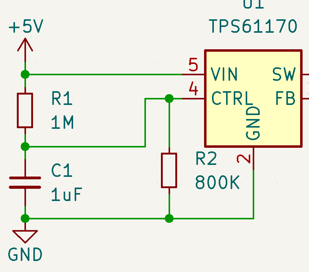
Schematic of the TPS61170 with the low pass filter. The 800K resistor is an internal pull-down and shown for clarity.
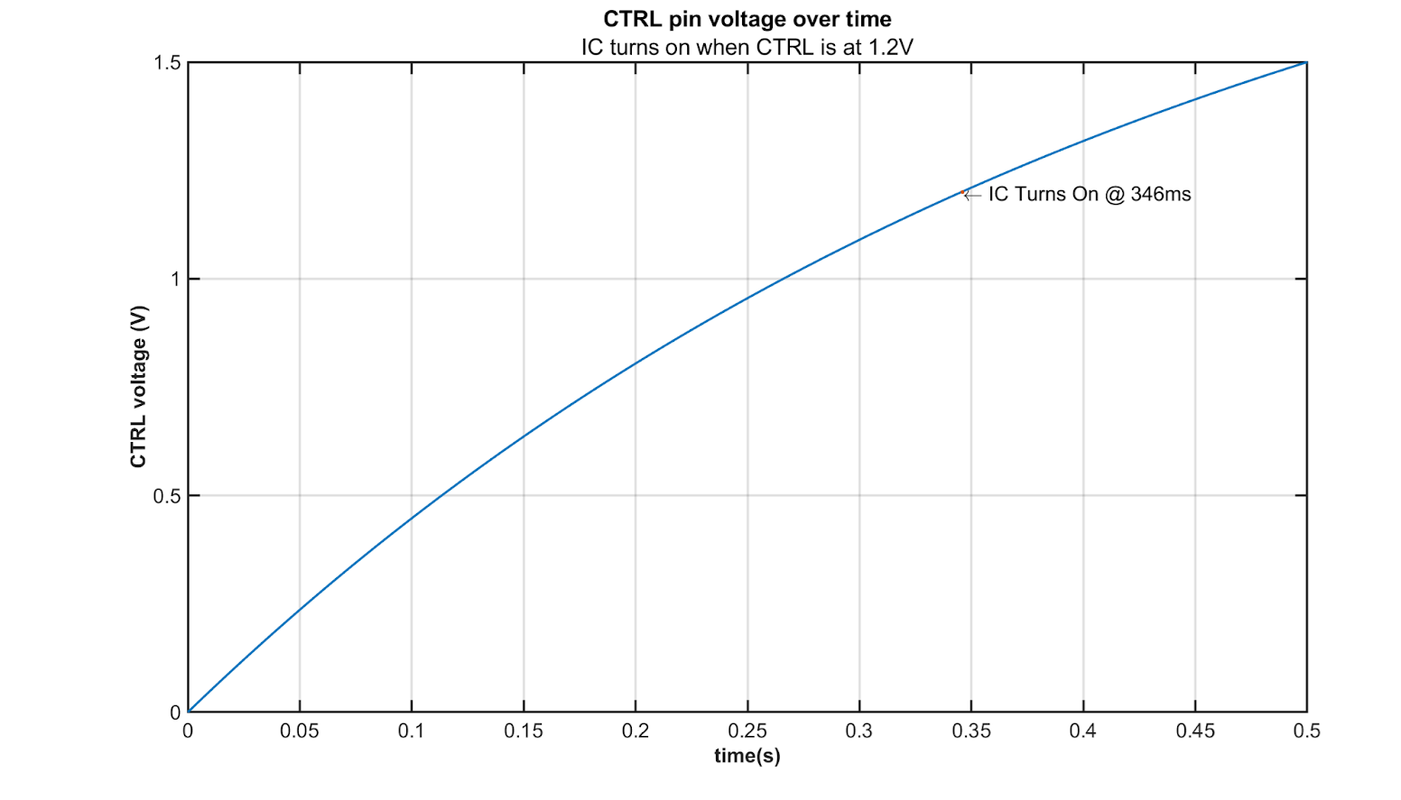
Simulation plot of the CTRL pin when a 5V Step input is applied. It shows the IC turning on at 346ms after 5V is applied.
02.02 - Capacitive Loads
Okay, so we know that it’s good to have bulk capacitors where the power entry is at. What would happen when it gets plugged in though? Let’s simulate it. Here’s a schematic. We have a voltage step to represent it being plugged in. Let’s say our wire resistance is 1 $m\Omega$ and we have a 1000uF capacitor hooked up to the circuit. When we turn it on, let’s measure the current across the capacitor.
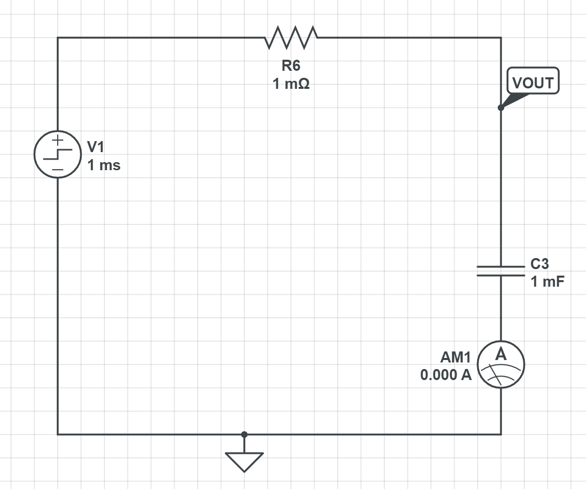
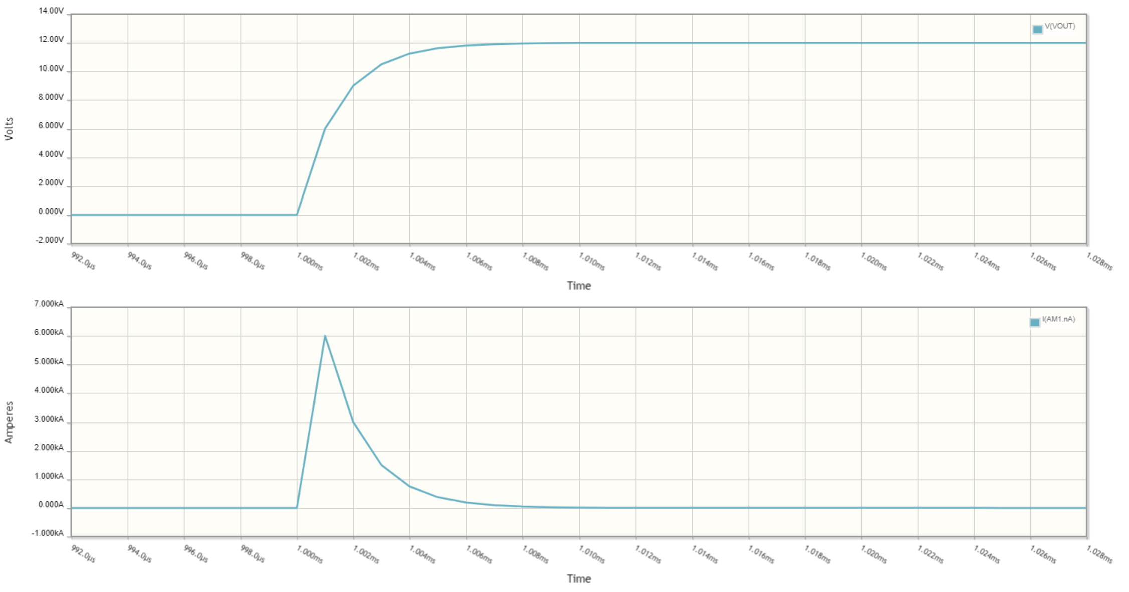
Let’s explain what you’re looking at. The top is the voltage at VOUT. It looks like a 1st order response, pretty typical for an R/C filter. What about the current waveform? It also looks pretty normal– we know that $I_C = C \cdot \frac{dV}{dt}$. In other words, the current through the capacitor is proportional to the change in voltage across it over time. The voltage change is quite high– it is a step after all! So the peak of the current draw is… 6kA! Yep. That’s 6,000 Amps of pure electrons, into your capacitor. You can guess why it’s called the inrush current. If you’ve ever heard a pop when plugging in old electronics to the wall, that’s what you’re hearing. The current through a capacitor when it’s plugged into something is enormous, and we must engineer a solution to not reduce the lifetime of capacitors every time it’s being plugged in. We’d need a way to control the speed at which the input voltage ramps (referred to as the slew rate) in order to control the inrush current.
The slew rate controlled switch
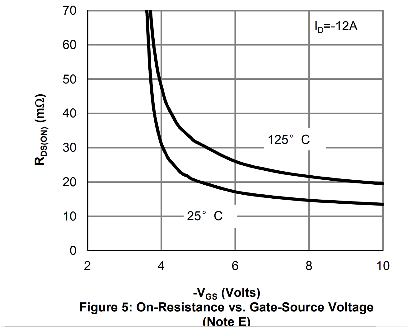
You might remember from the MOSFETs guide that $R_{DS_{ON}}$ goes from infinite to almost 0 as $V_{GS}$ is being increased. Here’s a graph of $R_{DS_{ON}}$ vs $V_{GS}$. Note that we’ll be referring to $V_{GS}$ as $ \vert V_{GS} \vert $ thereafter because it’s confusing to refer to a negative voltage on a P-channel mosfet.
If we can put a P channel MOSFET in series with the voltage step and slowly increase $ \vert V_{GS} \vert $ , maybe would use the high initial $R_{DS_{ON}}$ to slowly charge up the capacitor. Then, as the MOSFET turns on more, $R_{DS_{ON}}$ decreases to almost 0 and there’s no steady state loss using that system.
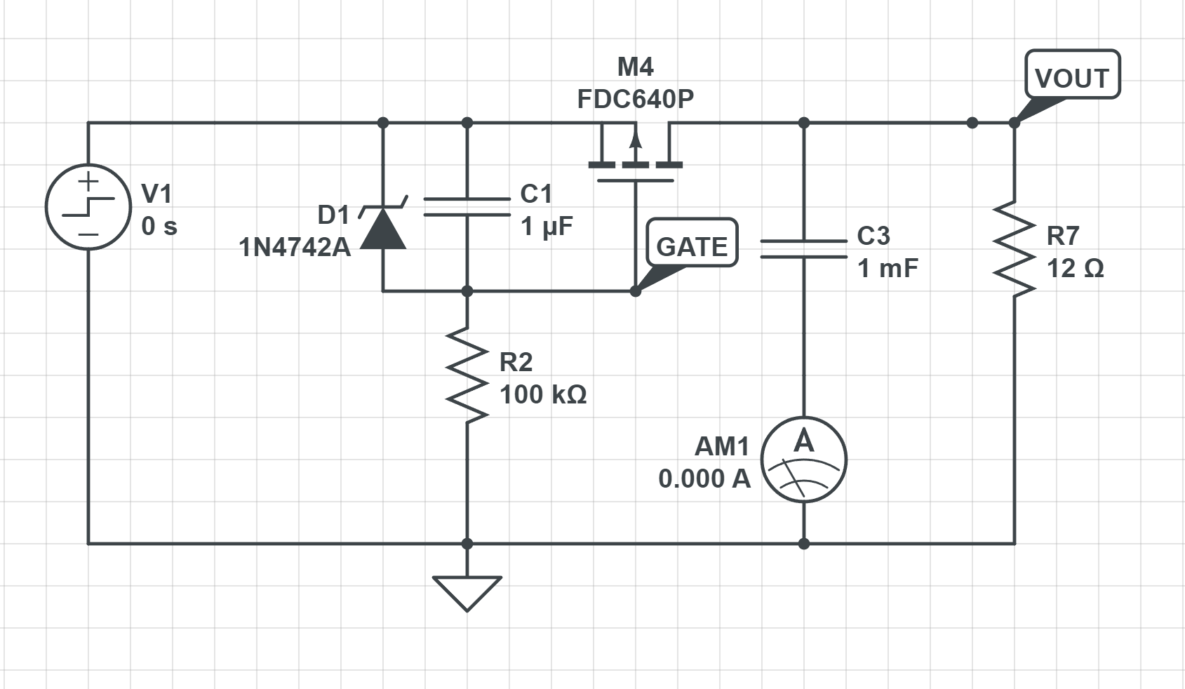
Here, we implemented just that. This circuit seems complicated, but let’s take a look at each part. Recall that the gate of the MOSFET draws almost no current, so the network connected to the gate can be analyzed without the MOSFET there.
Initially, the voltage step will be at 0V. This means C1 will have no charge across it. As the voltage steps, C1 will get charged through C1/R2. This forms a low-pass filter, so the gate voltage will slowly be ramped. The diode you see is a zener diode, and it clamps the gate-source voltage to 12V. This is because many MOSFETs cannot withstand a gate-source voltage over 20V. We know that the MOSFET fully turns on at 10V, and the zener diode won’t do anything until the gate-source voltage reaches 12V. So, the zener diode shouldn’t really affect the turn-on process.
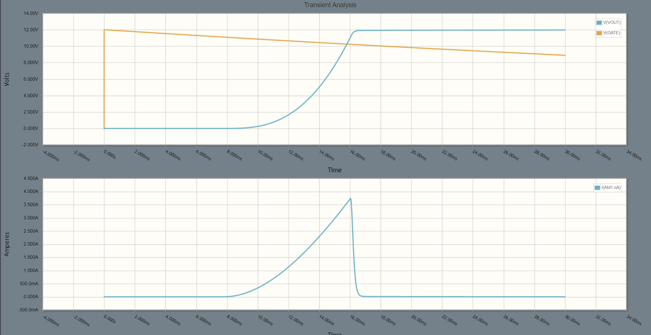
Let’s now simulate it! The orange line is the gate voltage. Remember, we’re looking at a P-channel MOSFET, so a larger $\vert V_{G} - V_{S} \vert $ means the MOSFET is more on. This happens when the gate voltage drops closer to 0V. We can see it ramps downwards as expected, and the large time constant results in a slow ramp. You can see when the MOSFET turns on– it’s when the blue curve ramps up. Since the slope of that blue ramp is controlled, the inrush current is now closer to 4A, which is much better for everything involved.
Let’s talk about some downsides to this solution. First off, it involves lots of parts. These parts need to be validated. If you want something simple to slap on, this may not be ideal if you need to test what time constant you need to avoid large current spikes.
The MOSFETs also feature body diodes, courtesy of our enemy the parasitic. It’s not possible to make a (3-terminal) MOSFET without the body diode. If you later find a way to do this, let us know, then patent it– you might be the next billionaire. For most cases the body diode doesn’t pose an issue, but if you’re doing a solution where both sides have power, you might get backpowering. Think of a battery being the load, and a charger being the input voltage. For this reason, a lot of devices with this problem put two MOSFETs back-to-back so the body diodes point in opposite directions and do not allow for current flow this way. Fun fact, many USB-C peripherals need this!
Image from TI SLVA948
The NTC Thermistor
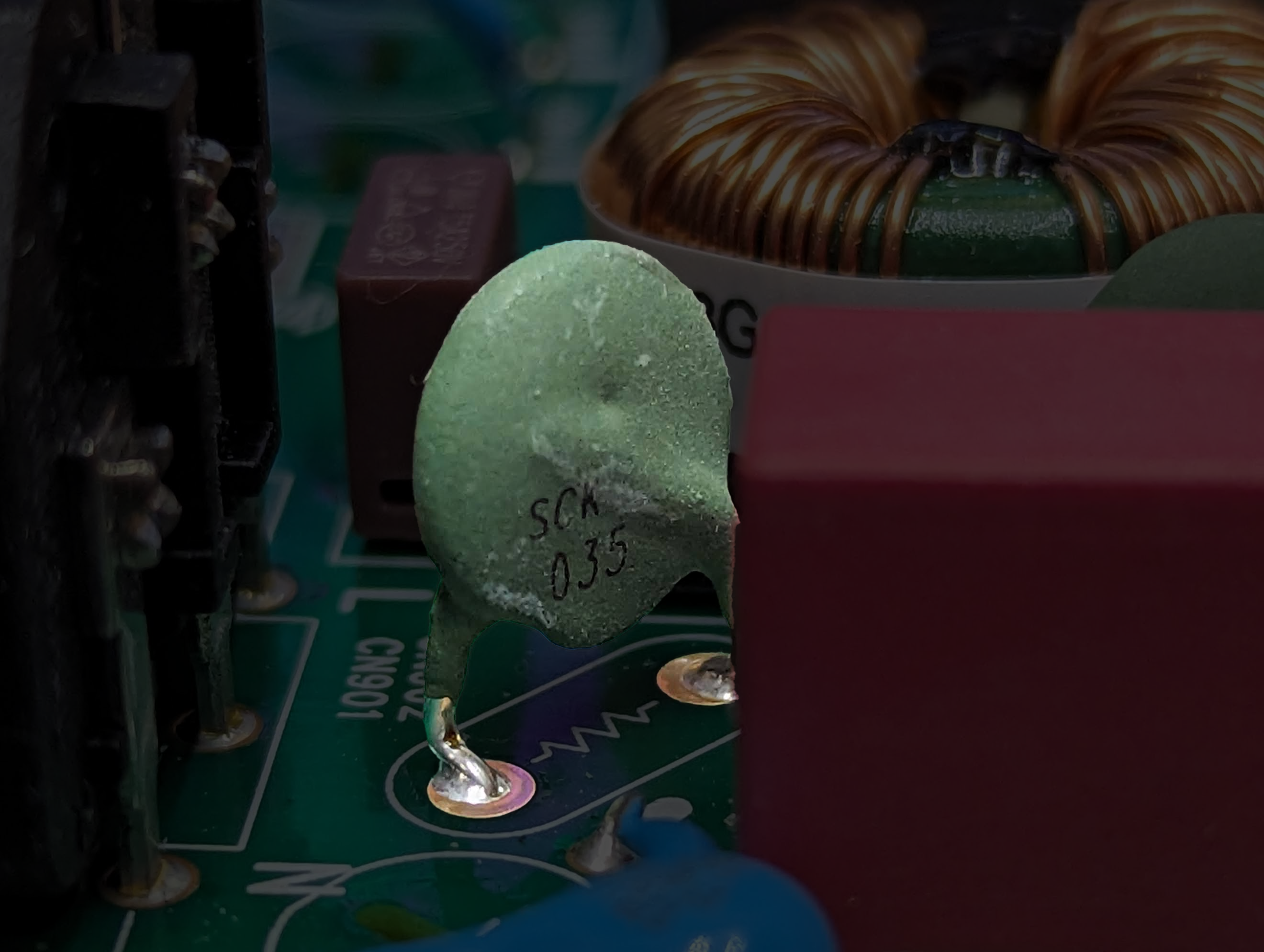
Image and editing credit: Winnie Szeto
There’s other devices that can also vary its resistance! This is a Power NTC thermistor. NTC standards for negative temperature coefficient, so its resistance decreases as the temperature increases. The “Power” name implies that this thermistor is able to dissipate more heat than most other thermistors. Most other thermistors are much smaller and can’t handle more than a few milliamps, whereas this thermistor can handle a few Amps.
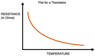
Image credit: Digikey
Here’s a typical plot of a thermistor’s resistance vs temperature. As you can see, as temperature rises, the resistance drops. It looks quite similar to the plot from the MOSFET! If we insert a NTC thermistor in series with the circuit and start it up cold, the initial resistance will be high, limiting inrush current. Once the circuit is on, we could find a way for the thermistor to heat up, reducing its resistance. Conveniently, it’s a resistor! This means that as current flows through the thermistor, it will heat up without us needing to do anything else. All we have to do is select the right size so the thermistor gets warm enough to lower its resistance, while not getting too hot and damaging itself. This solution is quite elegant and requires only a single part. However, it doesn’t work for quick plug/unplugs. The thermistor will stay warm when unplugged, meaning a 2nd quick plug-in will not be protected. This is quite a rare use case, and many AC -> DC power supplies are okay with this tradeoff and will often use a NTC thermistor for inrush protection. In fact, that picture is from a AC -> DC power supply! You can somewhat make out the AC plug on the left.
02.03 - Inductive loads
Inductive loads have the opposite problem. If inductors are quickly connected to a power source, it’s not a problem. Inductors are like massive trains. They don’t like instantaneous change. If you try to accelerate a train, it’s going to take forever to get moving. Same with inductors– if you attempt to run a current through an inductor with a constant voltage source, it takes time in order to push a current through the inductor. Once you get that train moving though, it’s going to be hard to stop. Trains take miles to stop because of how heavy they are. Now with the inductor, they can’t be unplugged from a current source. Inductors store energy by converting current flow to a magnetic field. When they’re unplugged quickly, this magnetic field collapses, and a current is forced through the inductor. The inductor doesn’t care if it’s disconnected, it will find a way to push a current through itself. This means that the voltage across the inductor can reach thousands of volts until something breaks and conducts current. This might be the air turning into plasma, or more often, it will kill a MOSFET. MOSFETs have (relatively) low maximum voltages, and they fail to a short when high voltage is applied. Once the inductor kills the MOSFET, it’s able to dump its energy into a current that flows through the killed MOSFET.
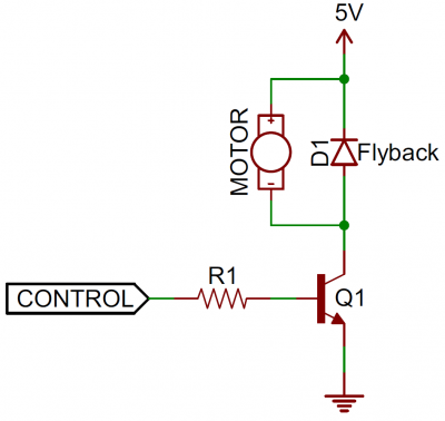
Image credit: Sparkfun
The solution is to place a diode in parallel with the inductor, but opposite to the current path. When the transistor is on, the current flows through the inductor (motor) and the diode is inactive. Once the transistor is off, the inductor’s collapsing magnetic field pushes a current in the same direction as when it was on, meaning there’s an electron build up on the +5V side. This leads to a higher voltage on the bottom node, and the induced voltage is able to push current down the inductor and up the diode in a loop. It’s like if you stopped the train by letting it move in circles.
Here’s a video that explains inductive load protection. The MOSFET isn’t destroyed because the energy stored in the motor’s inductive load is relatively small, and the MOSFET (specifically the body diode) is able to allow that current to flow.
02.04 - ESD
At one point or another, you’ve probably felt an electric shock. These shocks can typically be over 1000V of static! If it was to a doorknob or another non-electronic device, then it’s probably fine. You got a bit spooked, but that was about it. For electronics however, it’s a different story.
MOSFETs and other silicon devices are particularly sensitive to electric shock. It’s typically referred to as ESD (Electrostatic discharge). Here’s an image of what ESD-induced failure looks like. It will literally blow a hole in an IC! Often times, ESD damage can look like a short but have no physical damage to the package. They’re incredibly hard to identify because ICs are typically encased in a plastic resin. The pictures you see are likely from an optical and scanning electron microscope, and they’re likely only visible because Vishay is able to make a MOSFET without an encapsulate for testing purposes.
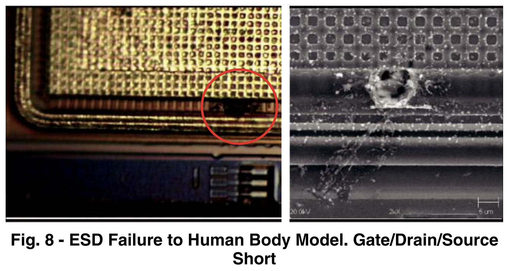
Image credit: Vishay
If we want to protect our devices, we would want a device that shorts the ESD energy to divert it away from the device it’s protecting. During normal use though, we would want this device to act like an open circuit so it doesn’t affect normal use. Let’s look at diodes. They act like an open circuit when the voltage is under the threshold voltage, and they allow large amounts of current to flow once the voltage across the diode is larger than the forward voltage.
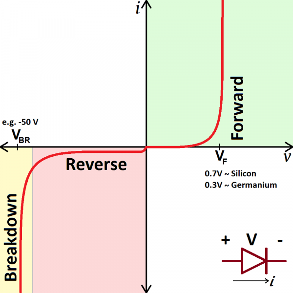
Image credit: Sparkfun
The diode’s forward voltage ($V_{F}$) is unfortunately stuck at 0.3-1V depending on the diode chemistry. It’s not possible to vary this voltage since it’s related to the chemistry of the diode. If we could vary the forward voltage though, it would be perfect for only turning on during large voltage spikes.
Let’s look in the opposite direction. There’s a very similar curve in the reverse region. The diode conducts in the opposite direction if the reverse voltage is beyond the breakdown voltage. The reverse conduction shouldn’t be a surprise since the voltage pushes current in the opposite direction. The problem with using this is most diodes will be destroyed if they go into reverse breakdown. Notice, most, not all.
Enter: the TVS and zener diode. The TVS (Transient Voltage Suppression) diode is great for fast and large voltage peaks. They’re specifically designed to protect against ESD and other short electrical energy pulses. They’re not ideal for continuous conduction however. If they’re conducting for too long at the same time, they may die.
Zener diodes on the other hand, are ideal for continuous conduction. Check out the zener diode (D1) that is being used in the slew rate limited switch. Let’s say V1 is a constant 20V. If the zener diode is a 12V zener diode, then the zener will start reverse conduction when V1 - GATE = 12V. Since R2 is quite large, the low resistance of the zener (~ 100 Ohms or so) is able to pull the gate voltage harder, ensuring (V1 - GATE) will never exceed 12V. This action is called clamping since the diode restricts the voltage to 12V and below. This is useful since if (V1 - GATE) exceeds 16V or so, then the MOSFET (M4) could be damaged.
For more information on what ESD protection to use for a specific application, check out TI’s guide.
02.05 - Logic levels
Often times, different ICs have different notions of what a “high” and “low” signal means. An Arduino Uno considers 5V a “high” output signal, and 0V a “low” output signal. A Teensy, ESP32, Raspberry Pi, and many more considers 3.3V a “high” output signal, and 0V a “low” output signal. In most cases, a “high” output from an IC is the input voltage of that IC. An Arduino Uno R3’s microcontroller is the ATMega328, which runs on 5V. In comparison, the ESP32’s microcontroller is the ESP32-D0WD, which runs on 3.3V. Some more advanced microcontrollers, like the IMXRT1062 on the Teensy 4.0, have a separate voltage input for GPIO (named VCC_IO). This allows for you to select whether the output high voltage is 1.8V or 3.3V. This still a lot to keep track of, and they may not work with each other.
On frying microcontrollers
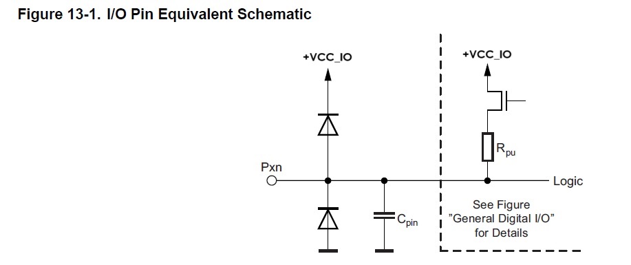
Image credit: Microchip
Here’s what a GPIO pin looks like internally. $C_{pin}$ is in the pF range, so we don’t have to worry about that for most circuits. You might recognize those diodes as ESD protection! That’s exactly what they do. Imagine if $P_{xn}$ was under 0V or over +VCC_IO. The diodes would turn on, protecting the logic signal from being out of range and damaging the microcontroller. For short events this works fine, but they’re not designed to handle an extra 2V for an extended period of time. Imagine if VCC_IO is 3.3V, and you’re pressing a button that connects $P_{xn}$ directly to 5V. You’d probably kill something! For this reason, we have to be careful of voltage levels to ensure they don’t damage anything. You do have a margin of ~ 0.3V due to the diode drop, but that should be used for a margin of safety and not as an excuse to push the input voltages to be higher.
Shifting voltage levels
The only safe case where you won’t cause damage is if your input signal has a lower high voltage compared to the IC logic voltage. For instance, a 3.3V signal will not kill a 5V-based Arduino Uno. But will the Arduino correctly interpret a 3.3V signal as high? What about a 1.8V signal?
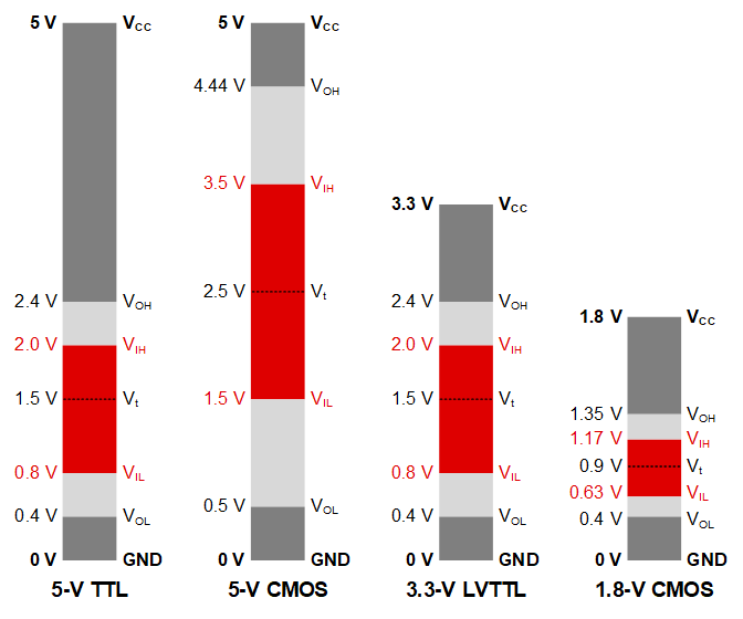
Image credit: TI
Here’s a chart of different thresholds by logic level type. An Arduino uses 5V TTL, most 3.3V devices use 3.3V LVTTL. But what are all those letters and numbers?
I/O refers to In or Out. H/L refers to High or Low. For instance, if we’re sending a 3.3V logic level signal, then the 3.3V sender would be required by this spec to output a high signal (VOH) of 2.4V or higher. If that’s signal is being received by a 5V TTL device, then it interprets an input voltage of 2.0V to be high (VIH). This means that if the voltage drop across the wire is under 0.4V (which it should) then a 3.3V LVTTL high signal can be interpreted correctly by a 5V TTL device.
The red region refers to the “I don’t know” region of the IC. If you were interpreting a signal using the 3.3V LVTTL standard and you saw 1.5V, is that high or low? It’s right in between, so ¯\ (ツ) /¯. If your logic level goes into this region, there’s no guarantee it will be interpreted correctly. This means if we’re trying to go from 1.8V CMOS to 5V TTL, we’d need something in between to “shift” the logic levels. If you’re shifting in a single direction from a higher voltage to a lower voltage, a resistor divider should work. In any other case, you’d need a circuit with lots of discrete components, or a IC designed specifically for logic level shifting.
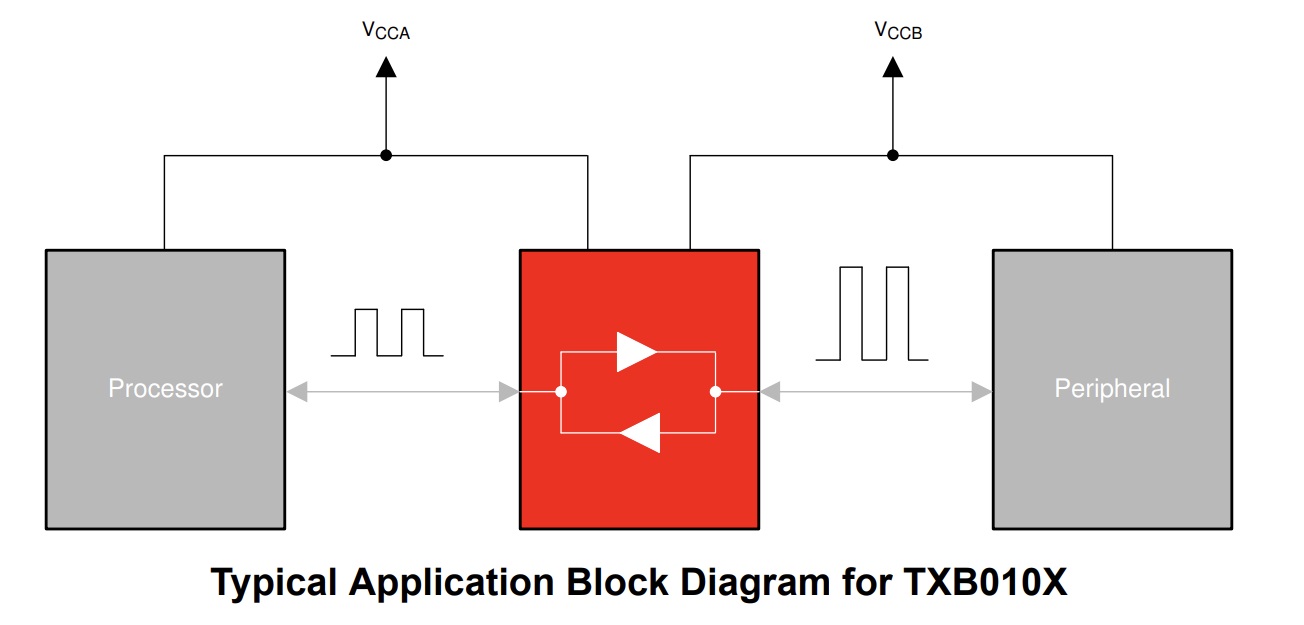
Here’s an application block diagram of the TXB010x from TI. The processor has a logic level VCCA, so the IC’s VCCA is connected to that voltage. On the opposite is a peripheral with a logic level VCCB. That voltage is fed into the opposite side of the IC. This allows the processor and peripheral to communicate at their respective voltage levels. This specific IC is bidirectional, means the processor or the peripheral can be the one sending the data. Other ICs differ– some are unidirectional, and some are built especially for protocols such as I2C. Be sure to identify what protocol you’re trying to logic level shift and ensure that the device you’re using for that purpose is able to shift that specific protocol.
For more on voltage levels, check out this video from TI
03 - Designing for testing and use
When designing a PCB that will be used by us, there’s a few things to consider. PCBs are inheriently more specialized than our other protyping methods such as breadboard, so we have to be intentional about things like testing, modifying, and human interaction.
03.01 Test points
With a breadboard, it’s so easy to stab a wire in a row and get a signal to measure. With PCBs, this isn’t as easy. Unless you add a point to probe, it’s going to be hard to probe. You can sometimes get away with sticking a probe on a component, but this is only true if the components are big enough. Let’s say we’re the Raspberry Pi foundation, and we need to test every single raspberry pi before it get shipped, and you’re making over a million a month. You won’t find technicians poking at resistors the size of dust particles. Rather, Raspberry Pi has put “test pads” on the bottom of their devices. They allow for an automated process where a machine can place the raspberry pi on a test jig to check signals and program it. You’ll want to consider the important test signals on your board, and add test point symbols to it in your schematic.
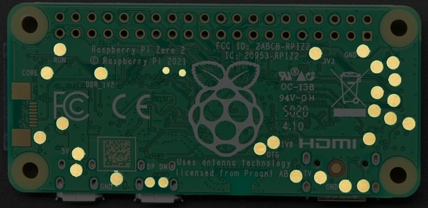 Image credit: Adafruit,
Editing credit: Winnie Szeto
Image credit: Adafruit,
Editing credit: Winnie Szeto
In contrast, let’s take the viewpoint of us– trying to debug a board. Unfortunately the limit of human hands per person is at two for most of us. This means probing multiple test signals will be difficult. This is why loop test points exist. They are a loop and you can hook an oscilliscope probe to it easily. Below is a development board from TI where they’ve added test points for ease of testing. Keystone makes a lot of test points in this form.
 Image credit: TI, Editing credit: Winnie Szeto
03.02 Jumpers
It may seem counter-intuitive to add 0 $\Omega$ resistors. Why not draw a wire? That resistor adds extra cost and complexity. But remember, we’re making a PCB, and drawing a wire means we can’t un-draw the wire without getting some cutting tools out. Jumpers make this process simpler, as making a different connection means re-soldering a resistor.
This is a 4-way jumper to select whether pin 1 on the bottom header connects to 1 or 2 on the top header. It may be a meme, but mixing up TX and RX in a UART implementation is very common. By using this jumper, you ensure there’s a way to fix a mixup without re-ordering a board.
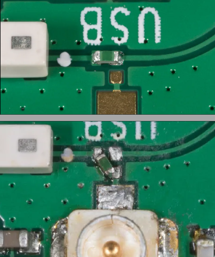 Image Credit: Brian Dorey
Here’s a jumper on a Raspberry Pi antenna. With a simple resistor re-soldering, a user can select to use the U.Fl connector for an antenna rather than the built-in antenna.
03.03 LEDs
Let’s imagine you’re designing a board for people who build their own computers. It would be incredibly difficult to probe test points on a motherboard that’s already in the hands of a user. Instead, you could add LEDs to the board. It makes it much more straight forward to identify exactly what’s going on and convey information.
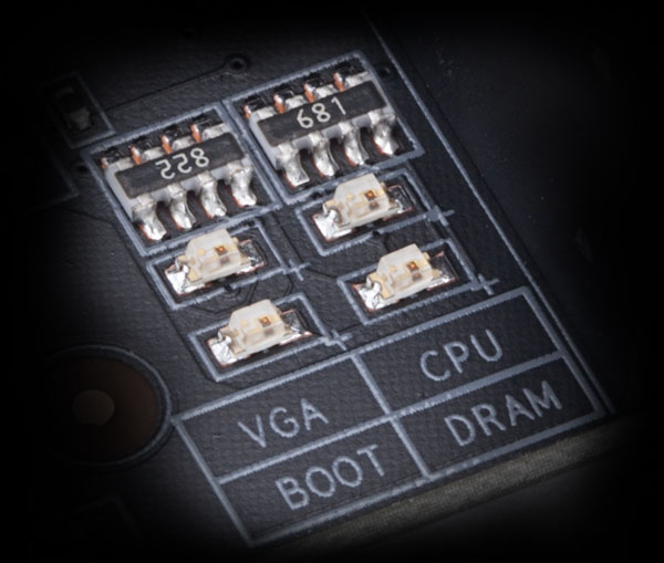 Image credit: Gigabyte
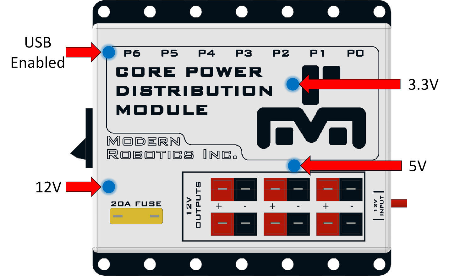
Here’s another example from Modern Robotics. If you’re old enough to remember this from FTC robotics, it’s a power distribution module. By simply looking at the LEDs, one can tell if it’s working properly. It’s fairly easy to place LEDs on a power rail, and it can save a lot of time when debugging.
03.04 Connectors, Buttons, Mounting holes
It’s extremely easy to forget about user interaction! Want an example? Our own demeo board does not have any buttons or mounting holes. We were under a tight timeline and… oops. We sent it in before considering how someone would use it. Don’t let this be you!
Buttons and mounting holes are pretty straight forward. Buttons come in many shapes and sizes, and we suggest you consider how your board is mounted and how stress will be relieved if you’re using them. For mounting holes, you may find solderable threaded inserts useful. The side without the black/yellow tape can be soldered down, and your board now has a threaded hole!
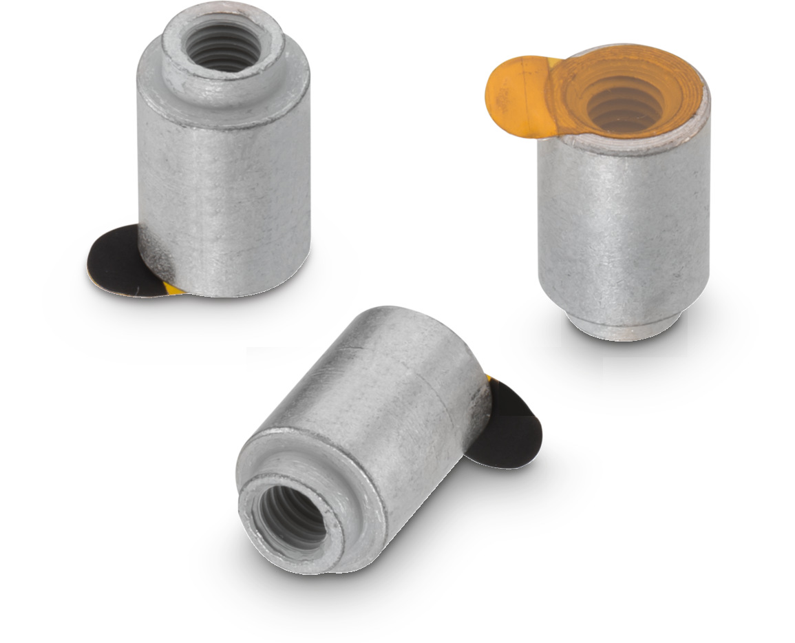 Image credit: Wurth Elektronik