Additional PCB Features
As you’re finishing up or reviewing your layout, there are some additional PCB layout features that you can implement for certain board needs. This section will go over these additional features, but they are not necessarily actions you may need to take for your board.
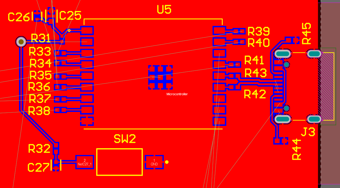
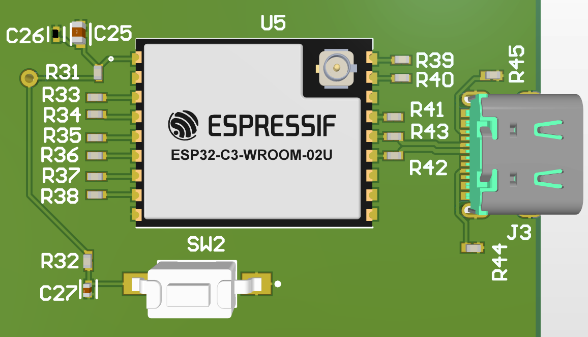
Microcontroller Layout Example
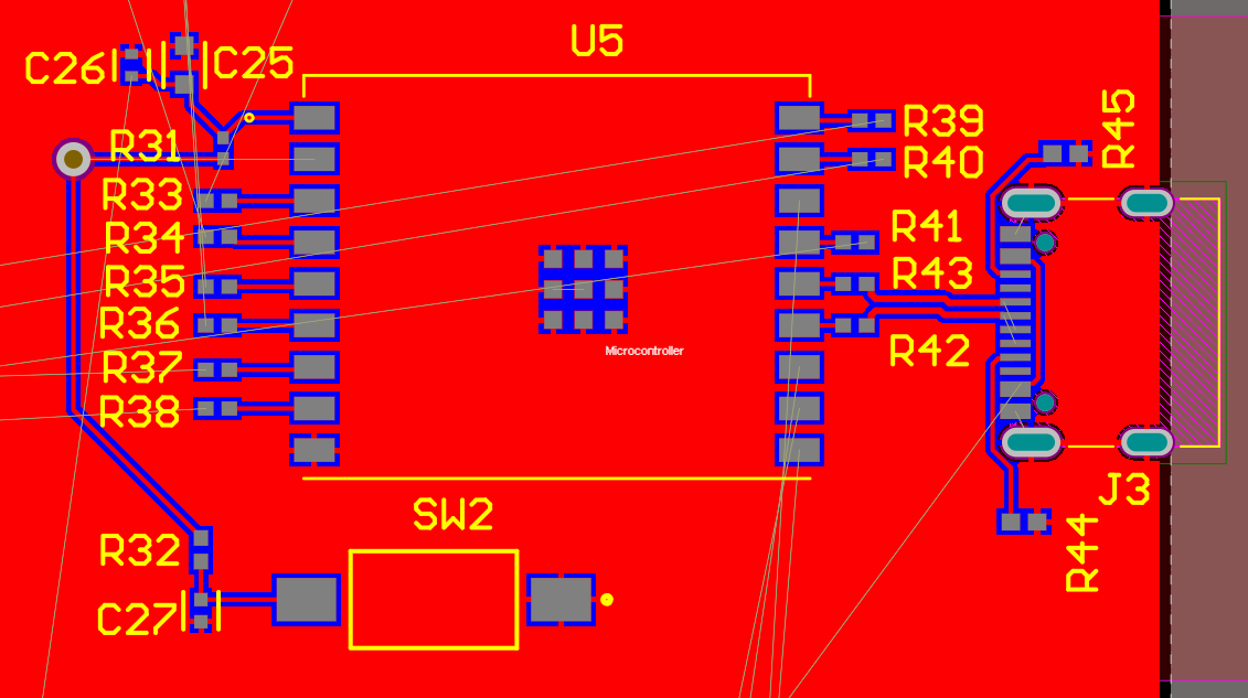
As an example, we’ll use the partially-finish layout for the ESP32 microcontroller and apply the features to it.
3D view of the partially-finished ESP32 layout.
Soldermask Removal
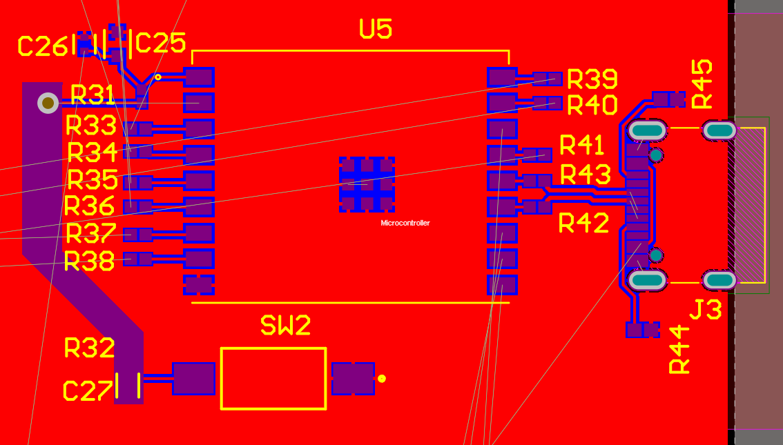
Sometimes its necessary to remove the soldermask from a section of the board. For instance, transmission lines carrying very high-frequency signals will often have the soldermask covering them removed in order to reduce the effects the soldermask causes to the characteristic impedance via the fringing fields.
The top and bottom soldermask layers in most PCB EDA tools are negative layers, meaning that drawing something on the layer denotes where soldermask should be removed. If nothing is drawn on the soldermsak layers, then soldermask will cover the entire board. This is why you will see drawings of footprint pads on the soldermask layers as they must be exposed copper.
In our microcontroller example, we can draw a region around the leftmost trace on the top soldermask layer to have it be bare copper.
And here’s how the board would actually look like.
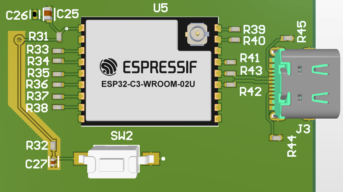
In our board, we have no reason to do this, so put the soldermask back to how it was when you are done playing with it.
Viewing Paste Layer
As a way of efficient and reliable PCB assembly, a stencil is used to apply solder paste evenly over all of the SMT footprint pads on the board. Therefore, in order to produce an appropriate stencil, we need to define what and where the stencil cutouts will be.
The solder paste stencil cutouts are defined by drawings on the top or bottom solder paste layers (since components will only be on the top side of the board, only the top solder paste layer is applicable).
Luckily for us, nearly all of the SMT footprints pads - which require solder paste - should already have the solder paste layer configured for them in the footprint appropriately. We can see this for the microcontroller layout if we highlight the top solder paste layer (look for the grey rectangles covering all of the SMT pads).
Design Rules Check
The design rules check (DRC) is the layout version of the ERC you used in the schematic. It will compare the layout you created with the DRC rules you set prior to board layout. Performing and addressing DRC issues is the final crucial step to ensuring that the board can be properly fabricated.
Altium DRC
To run DRC in Altium, go to Tools->Design Rules Check.
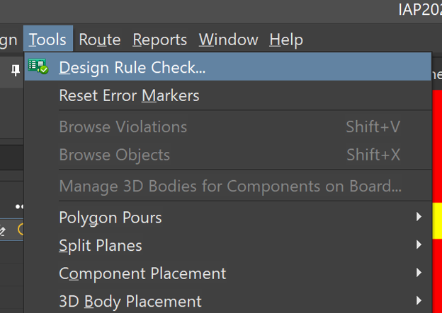
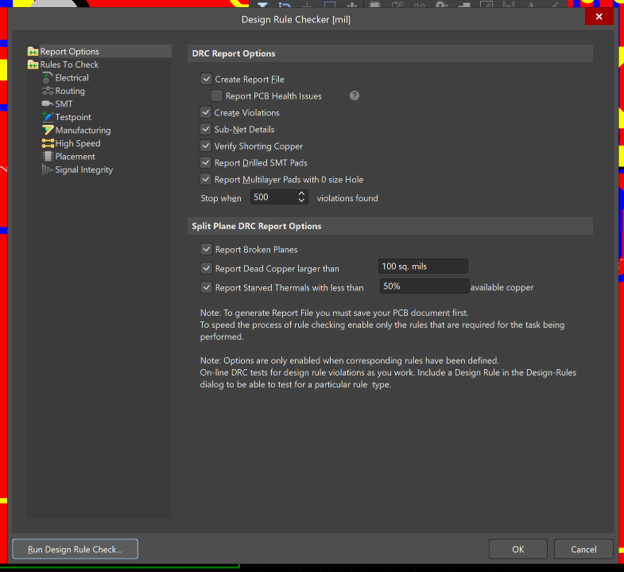
This will then show the DRC menu. We can leave the default options and run it.
Afterwards, a Design Rule Verification Report should pop up (if one doesn’t, make sure the Create Report File option is selected in the previous DRC options menu). The Design Rule Verification Report, as well as the Messages panel, will show all of the rule violations found in your layout. By clicking on each of the errors, you can jump to the location of the DRC issue to quickly resolve them.
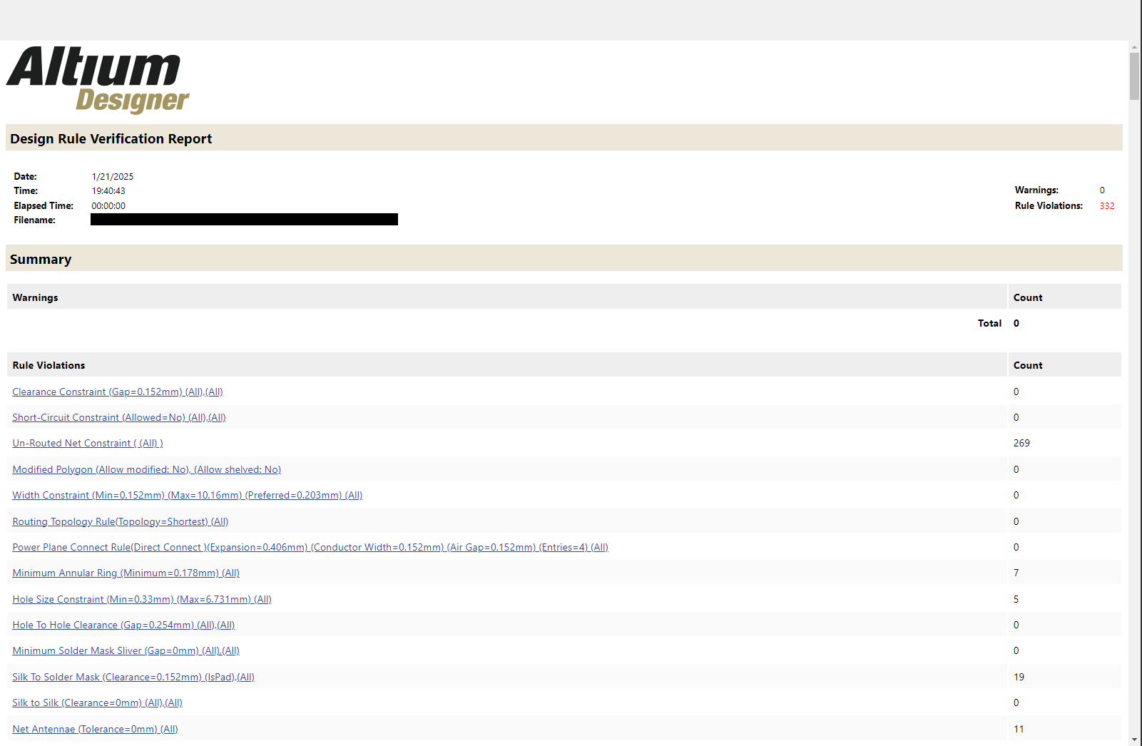
Some DRC warnings are derived from issues inherent to the component footprints used. These can only be resolved by adjusting the footprint accordingly (just like with the ERC warnings that were inherent to the symbols being used). Luckily however, the component footprints provided for layout have been previously verified to be successfully manufacturable, so DRC warnings that caused by features within a component footprint can be ignored. Note that you should pay special attention to whether a DRC warning is inherent/within a component’s symbol, in which it can often be ignored, or if it is caused by the interaction of multiple parts or features (e.g., traces, holes, pours), in which it must be resolved.
KiCad DRC
To run DRC in KiCAD, go to Inspect->Design Rules Checker.
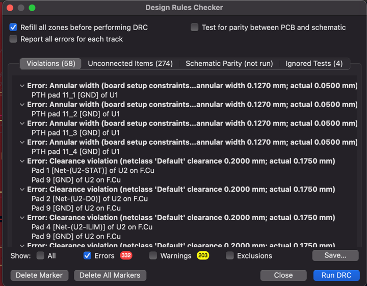
This will then show the DRC menu. We can leave the default options and run it. A list of errors and warnings should pop up as shown below. This list will have all of the rule violations found in your layout. By clicking on each of the errors, you can jump to the location of the DRC issue to quickly resolve them.
Some DRC warnings are derived from issues inherent to the component footprints used. These can only be resolved by adjusting the footprint accordingly (just like with the ERC warnings that were inherent to the symbols being used). Luckily however, the component footprints provided for layout have been previously verified to be successfully manufacturable, so DRC warnings that were caused by features within a component footprint can be ignored. Note that you should pay special attention to whether a DRC warning is inherent/within a component’s symbol, in which it can often be ignored, or if it is caused by the interaction of multiple parts or features (e.g., traces, holes, pours), in which it must be resolved.
Common DRC errors
| Rule | Explanation | Resolution |
|---|---|---|
| Clearance | Components or features are too close together | Move violating features further apart |
| Short Circuit Constraint | Multiple different nets are electrical connected to each other | Remove/separate the copper causing the unwanted connections |
| Un-Routed Net Constraint | A net associated with multiple footprint pads is unconnected (an airwire still exists) | Route a trace or copper pour between to connect the pads and complete the net |
| Modified Polygon | A polygon or copper pour was previously poured but changes to the board have occurred that require repouring | Repour the polygon or copper pour |
| Width Constraint | PCB feature (typically a trace) is in violation of width rules | Adjust the width of the PCB feature to be in compliance with the width rules |
| Minimum Annular Ring | The width of the copper ring surrounding the hole for a via is too small | Increase the width of the copper ring (i.e., annular ring) |
| Hole Size Constraint | Hole diameter violates hole size rules | Adjust hole size to be in compliance with hole size rules |
| Hole to Hole Clearance | Holes are too close to each other | Separate violating holes further apart |
| Minimum Solder Mask Sliver | The width of soldermask in the violating area is to small | Separate the features that require removal of soldermask (typically footprint pads) further apart |
| Silk to Solder Mask Clearance | Distance between the start/end of soldermask and a silkscreen print is too small | Increase the distance between the soldermask start/end boundary and the silkscreen print |
| Silk to Silk Clearance | Silkscreen prints are too close to another | Separate violating silkscreen prints |
| Net Antennae | One end of a trace is routed to a pad, but the other end is not (left unconnected, forming an antenna) | Route the trace to a pad or delete the trace if not needed |
| Height Constraint | Maximum height of components on board | No height constraint; can be ignored |
Bill of Materials
The bill of materials (BOM) is simply a spreadsheet that houses all of the required components for the FM radio (including those that are not soldered directly to the board, such as the speakers and batteries) and includes important information, such as:
- Reference Designator
- Component Value
- Quantity
- Manufacturer Part Number
- Supplier Part Number
- Cost
Ensuring that the BOM is completely accurate is critical for ordering parts. Every PCB EDA tool will allow one to automatically generate a BOM (based off the components included on the board) and allow verification of it.
Altium BOM
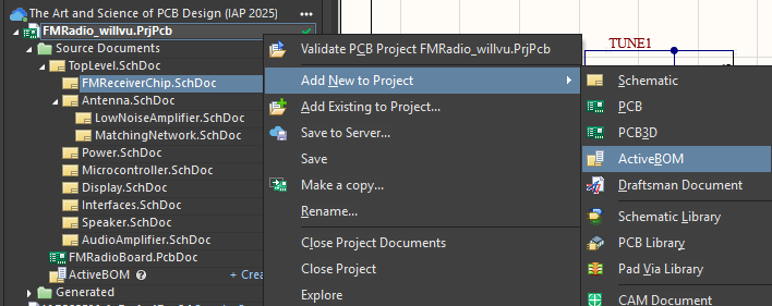
Begin by adding an ActiveBOM document to the project.
Now we can view the entire BOM. Notice how components with the same values are grouped together. To view the value parameter specifically, the Value column can be added.
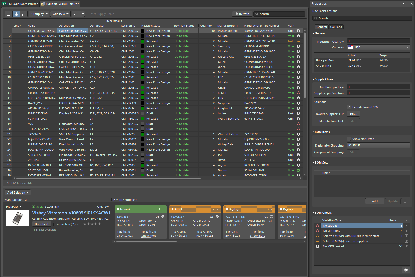
Within the ActiveBOM, follow this Altium guide for adding solutions to each component (if one does not exist already). All solutions should have DigiKey as a supplier. Adding solutions refers to assigning a real component (with a manufacturer number and that can be ordered in the quantities that are required from a supplier) to each component on our board/schematic. A video guide by Altium is also available.
Most parts from the library should automatically have a solution. One exception is the handful of generic parts (such as the RES0603 and CAP0603 parts), which you may have used and just changed the value for. Be careful of non-generic parts that you might changed the value for. Changing the value does not change the part solution, so any parts that you changed the values for will have wrong solutions.
When your BOM verification is finished and each component is orderable from DigiKey, you should have green checkmarks next to each component row. Now, your BOM is complete and can be ordered from DigiKey.
KiCad BOM
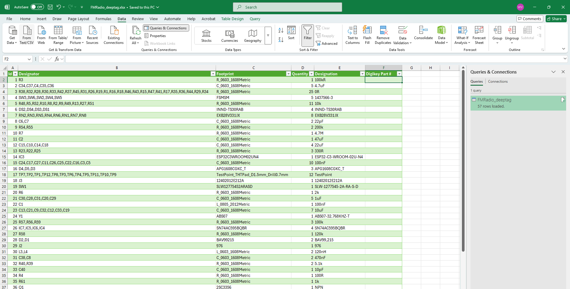
Before we can generate the BOM, we need to assign part numbers to all of our symbols that we used in the schematic. Head to Tools->Edit Symbol Fields. This pulls up a table of all of the symbols we placed and their properties. We will use assign two properties, Manufacturer and Manufacturer PN, to all of the symbols. If you look at the table list of columns on the left side, you should already see entries for Manufacturer and Manufacturer PN. Check Show Column for both of these.
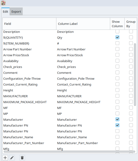
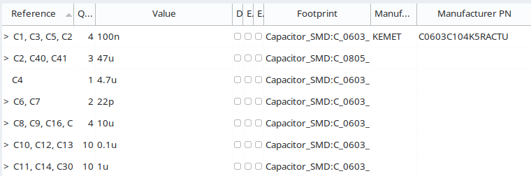
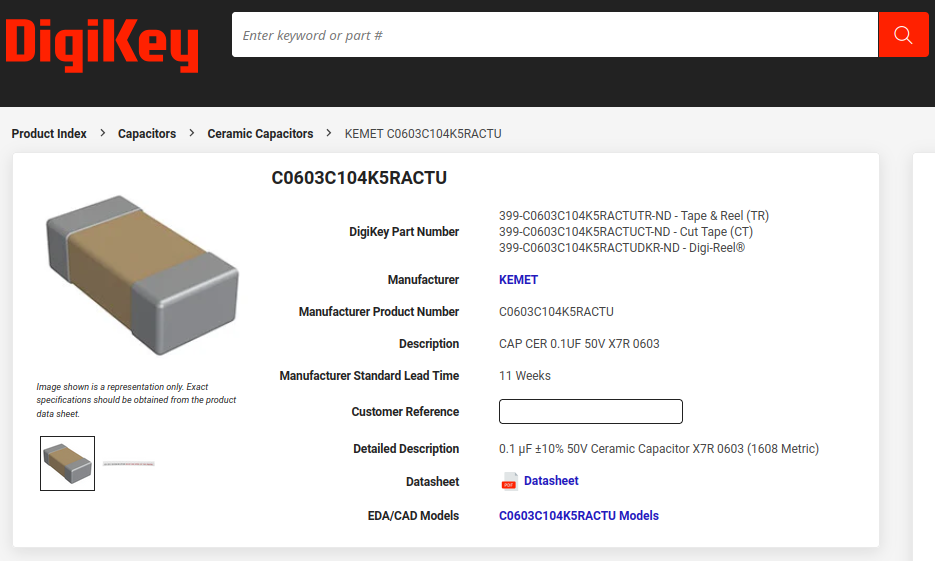
Now comes the important step. Go through each component and assign an appropriate Manufacturer and Manufacturer PN. For 2-pin chip passives, use the footprint and value to help search for the appropriate part in DigiKey. For example, for the first C1, C3, C5, C22 row in the image below, the footprint and value indicate that a “0603 100n capacitor” should be searched for in DigiKey. Using the filters to search for the appropriate Package/Case and Capacitance in this case will give much better results than using the general search field. Most of the parts that have the correct value and package will work fine, but make sure that the capacitors have a suitable Voltage rating, and maybe consider whether their Temperature Coefficient is appropriate. If you have questions about whether a part is appropriate, ask somebody from the course teaching team. When you have found a suitable part, fill out the Manufacturer and Manufacturer PN in KiCad, and make sure to save frequently.
For non-generic passive chip components (such as ferrite beads) and ICs, the value field to the manufacturer part number of the component, which can be directly searched for in DigiKey. Parts from the class symbol library should have the Manufacturer and Manufacturer PN already filled in. After filling doing this for all of the parts, make sure forward annotate (it’s always a good idea to commit your repo before using tools like annotation that can mess up your whole project).
Now we are ready to export the BOM. Head to Tools->Generate Bill of Materials which will generate a .CSV file containing the BOM.
Go to DigiKey myLists, where we will look up all of our parts and get the appropriate DigiKey part numbers. Select Upload a List and upload the BOM that you exported. Assign the correct mappings to each column. The columns that matter are Quantity, Manufacturer Name, and Manufacturer Part Number.
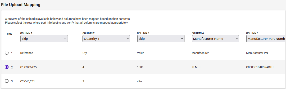
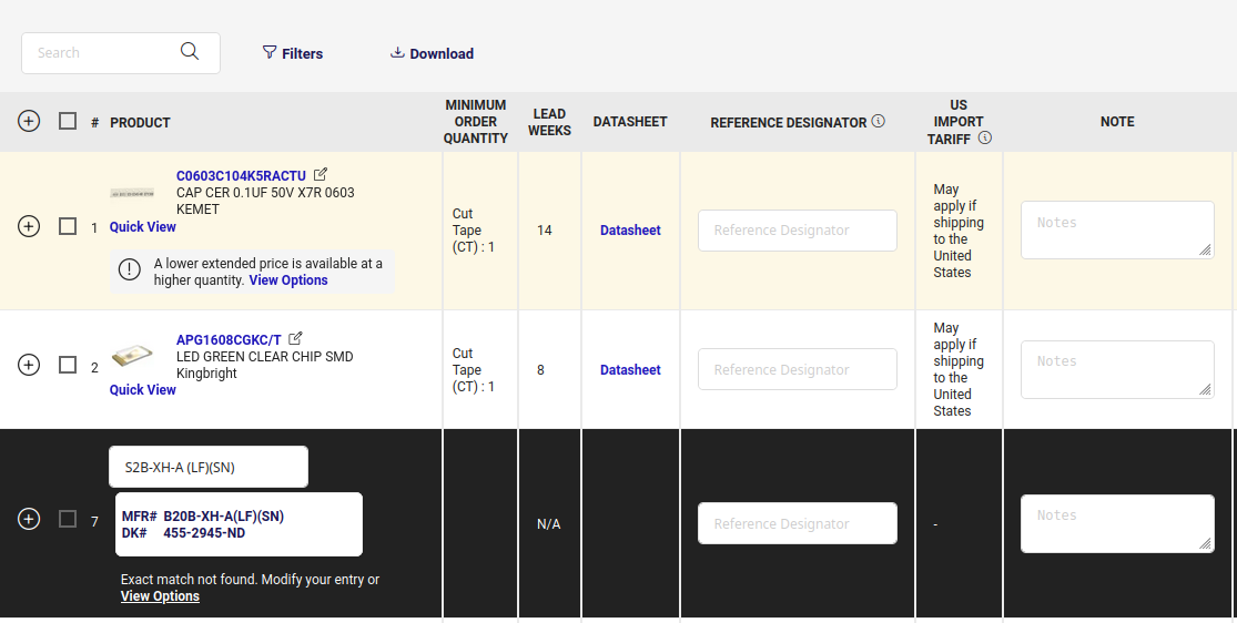
Now, press Continue, and you will be taken to a page that shows the parts that DigiKey found. Make sure that all of your parts had matches found. For example, in the image below it did not find the S2B-XH-A (LF)(SN) part, so an suitable substitute would need to be found. Once everything has matches, Download it from DigiKey.
Finally, open your BOM and DigiKey download in Excel (note that you may need to open a new Excel spreadsheet and open the BOM .CSV file using the Data->From Text/CSV option and specify the delimiter is a semicolon). Afterwards, create a column named Digikey Part Number in the BOM, which will hold the orderable DigiKey part number for each component. Copy the DigiKey part numbers from this download into your BOM (be careful of column order).
Fabrication Files
The final step to the PCB design process is generating the output fabrication files necessary for a PCB fabricator to make our board.
Gerbers are a common set fabrication files that describe exactly how the board should be created and are used by many PCB fabricators. In this section, we’ll create the Gerber files for our board as well as the schematic prints and BOM file.
Generating Gerber, Schematic Prints, and BOM Files
Altium File Generation
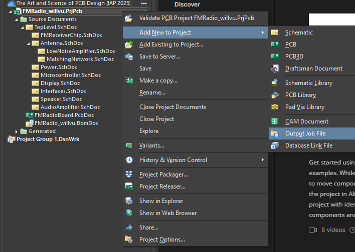
We’ll begin by adding an Output Job File to our project. It’ll allow us to generate all of our output all at once.
Next, we’ll add a Gerber X21 output. Assign its data source to be [PCB Document], but assigning it to be your FMRadio_[your kerb].PcbDoc PCB document will also work the same.
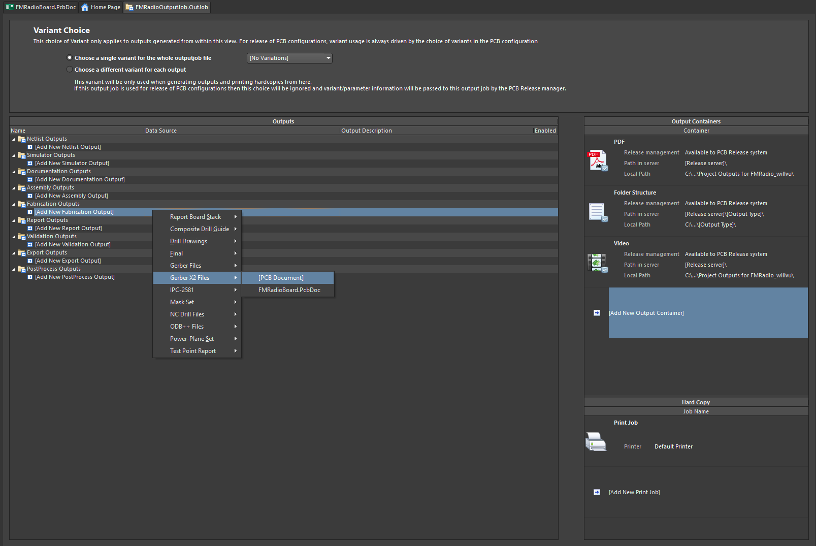
Right-clicking the Gerber X2 Files output row and clicking Configure... will allow us to adjust the options for the Gerber X2 file output.
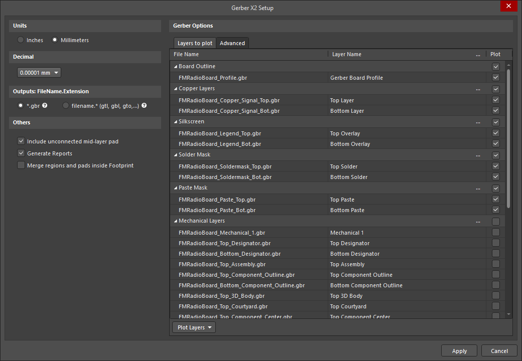
Keep the defaults and hit Apply.
Afterwards, add the Schematic Prints and Bill of Materials outputs. Once we have defined the three outputs, we need to assign them to an output containers (i.e., describe what format they should outputted as). Selecting the Folder Structure output container, enable the Gerber X2 Files and the Bill of Materials. Then, selecting the PDF output container, enable the Schematic Prints. A green arrow should correspondingly point from the outputs to their enabled output container when an output container is selected, as shown below.
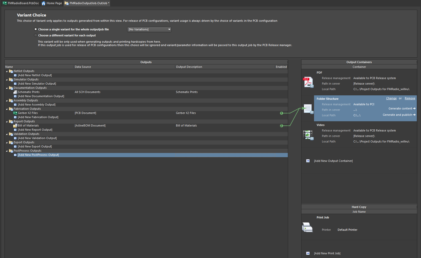
Finally, to generate the outputs, select an output container and click Generate Contents. The output container will then generate its associated output files as free documents in the project.
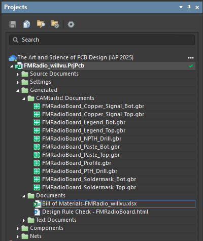
- Gerber X2 files will be in the
Generated->CAMtastic! Documentsfolder. - The Bill of Materials Excel spreadsheet will in the
Generated->Documentsfolder. - The PDF schematic prints are not shown in Altium Designer
Finally, find your generated Gerber X2 files in Windows File Explorer (it should be in directory similar to ...\FMRadio_[your kerb]\Project Outputs for Free Documents\GerberX2) and ZIP archive the GerberX2 directory. This ZIP file is what we will submit to PCB fabricators.
KiCad File Generation
You should have already generated your BOM as part of the KiCad BOM section.
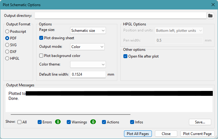
To generate schematic prints, use File->Plot....
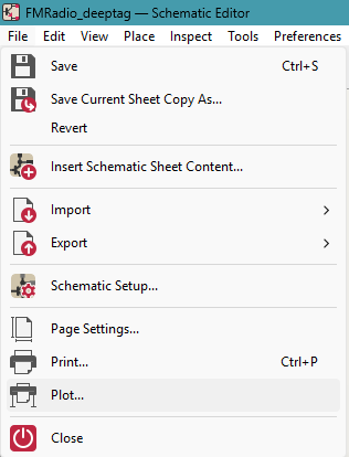
And Plot All Pages of the schematic as a PDF.
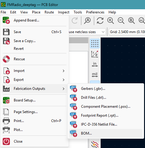
Finally, to generate our Gerber files head to File->Fabrication Ouputs->Gerbers (.gbr)...
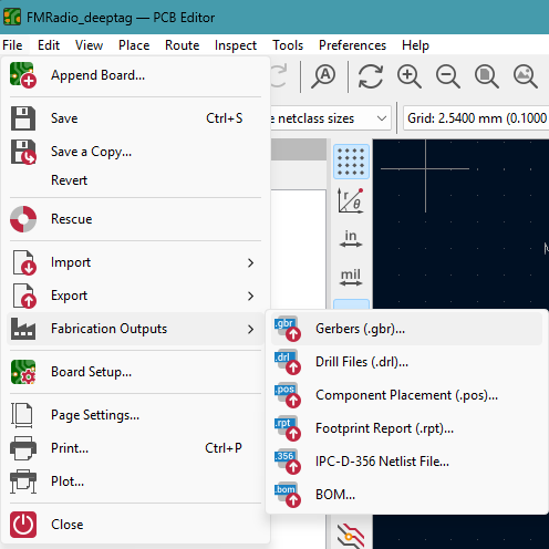
Afterwards, create a “Gerbers” folder in your project’s file directory and, in the Gerber plotting menu, assign the output directory to be that folder. Keeping the defaults, hit Plot and you should be left with Gerber X21 files in your “Gerbers” folder.
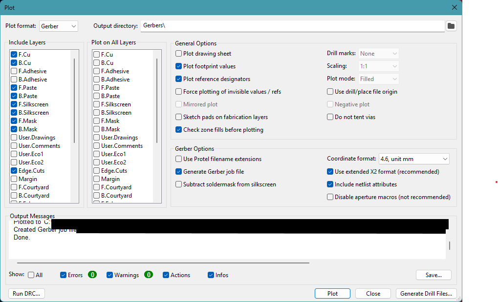
Find your Gerber X2 files and ZIP archive the folder containing them. This ZIP file is what we will submit to PCB fabricators.
Ordering Board
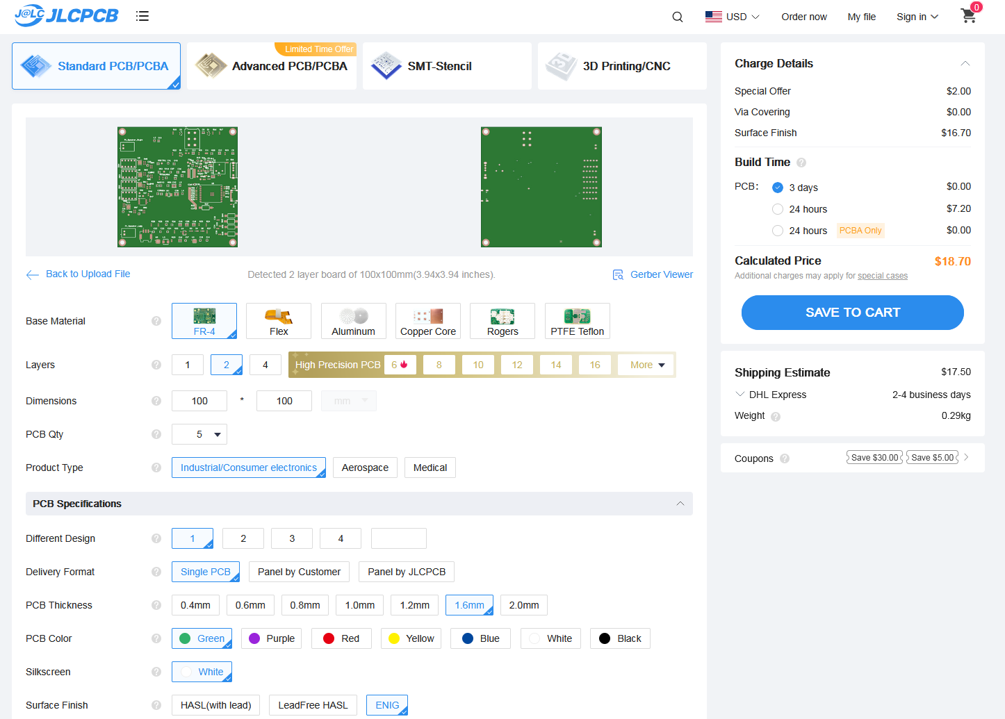
Now you can order your board to created at most PCB fabricator just by uploading the Gerber X2 zip file you created. Try it out with JLCPCB and use their online gerber viewer to check that your files uploaded correctly. After selecting ENIG as the surface finish, the cost should be about $20 without shipping.
Submission
Congrats! You’ve finished an entire board design for the FM radio project from the block diagram all the way to ordering the board.
Please submit your final fabrication files on this form by midnight Friday, 01/23/2026. The final required fabrication files are:
- Schematic prints (PDF), which should contain all of the schematic sheets as single PDF document.
- Bill of Materials (Excel spreadsheet), which should for each component, at a minimum, contain associated reference designators, quantity, and an orderable DigiKey part number.
- Gerber files (ZIP archive), which should have been successfully viewable after uploading into JLCPCB for a quote.
If you are having issues or are of need of an extension, please let the course staff know on Piazza.