Installing Altium Designer
The first step is to Install Altium Designer and complete the additional online workspace setup instructions if you have not done so already. Lab assistants can immediately add you to the Altium workspace if you are not currently a part of it
Creating a Folder in the Altium 365 Workspace
Once you’re added to the Altium 365 Workspace you should get an email with instructions to add the workspace to your Altium Installation and a link to the online Altium 365 workspace.
Go to the course’s Altium 365 workspace and sign in. Then click Projects, head inside of the “Projects” folder, and then click New->Create Folder.
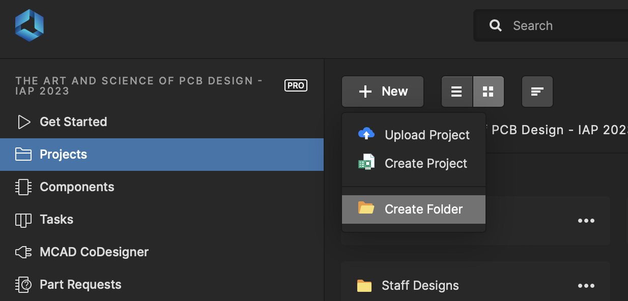
Create a folder and name it with your kerb.

Afterwards, create a project in your folder via New->Create Project and name it as FMRadio_[your kerb].
Once you connect to the Altium workspace in Altium Designer software itself, you should see the course’s workspace and your project within it.
Here’s another Altium 365 tutorial
Introduction
This lab is a super simple, super short lab! It’s basically just to get you familiar with the following in Altium Designer.
- Project Structure
- Schematic Capture
Creating a Block Diagram
The first, most important step in putting our electrical system into a schematic is first creating the top-level schematic (or block diagram). This is like the system-level block diagram that was discussed in lecture 01 except that it contains more detail about how the electrical device will actually work and is located at the root of our schematic sheets.
Having this top-level schematic is crucial to ensuring that we can effectively keep the whole system structure of the FM radio in mind as we create it. Doing so also allows us to break down the schematic design into separate parts (e.g., amplifier, speakers, power), which makes our life a whole lot easier
Top-Level Schematic Sheet
Within your FMRadio_[your kerb] project in Altium Designer, create a new schematic and save it as TopLevel.SchDoc.
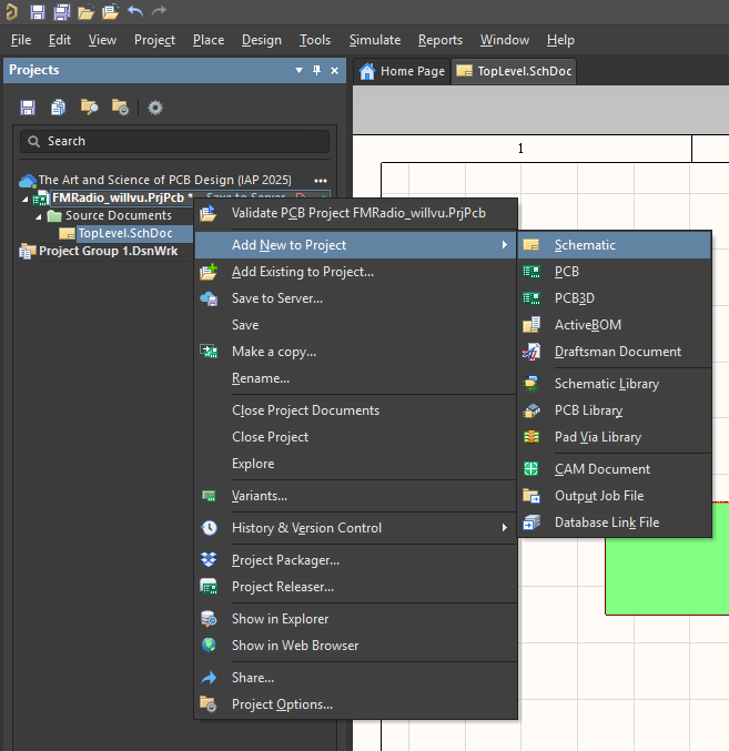
Next we’re going to build out the block diagram with all of its different parts.
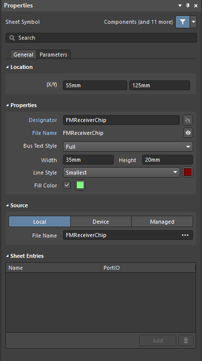
Within the floating quick access toolbar (right-clicking the symbols brings up the dropdown), select Sheet Symbol and add one to the schematic sheet. Afterwards, edit both the reference designator and file name to what block the sheet symbol is to represent. In this case, let’s have it be the FMReceiverChip. (you may want to turn off the visibility for the reference designator so the name doesn’t appear twice).
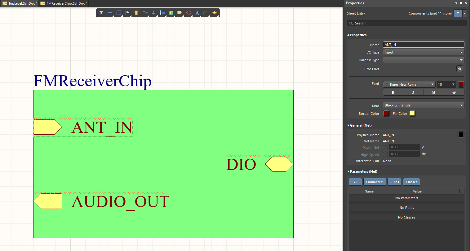
Now, we need to add ports to the block in order to connect it to other sheet symbols. In Altium, these ports are known as Sheet Entries and can be found in the same dropdown as where we found the sheet symbols.
Right now, we don’t know exactly what ports we need to have on each sheet symbol, and we don’t need to. We should, however, make sure we create the major connections and we can add additional sheet entries later on when we build out each block on the schematic.
For the FMReceiverChip sheet symbol, let’s add an antenna, speaker, and digital I/O port to it. Make sure to assign the I/O Type of each sheet entry to Input, Output, and Bidirectional, respectively. This allows Altium to help makes sure that we connect ports correclt (i.e., warn us if we connect an input to another input on accident). Also, you’ll notice the red squiggly lines above each sheet entry - this is part of Altium’s real-time electrical rules checker (ERC) and its warning us that the sheet entries aren’t connected to anything currently.
With one block down, let’s complete the whole block diagram! Hopefully in doing so, you’ll get an intuitive understanding for how the whole FM radio will be set up.
Notice that we had adjust the ports on the FMReceiverChip to have two speaker output ports (one for the left and right speaker) since we want stereo audio. Building out these top-level diagrams/schematics helps us realize such discrepencies.
Also, with these sheet entries it becomes easy to duplicate identical circuits - without having to draw them out twice. Just copy and paste the sheet entry. Such is the case with the left and right stereo audio paths.
Finally, notice how the Power block is not connected to anything. In theory, since it is the power block, it should connect to every other block - but that would make the whole schematic quite messy. So instead, in Altium (and all other EDA tools) power connections are considered global nets, which means that they connect to each other across the schematics and blocks without the need for explicit ports. This is just like how the GND symbol always implicitly connects to other GND symbols in a drawn schematic. Therefore, the power block just needs to exist and doesn’t need any ports
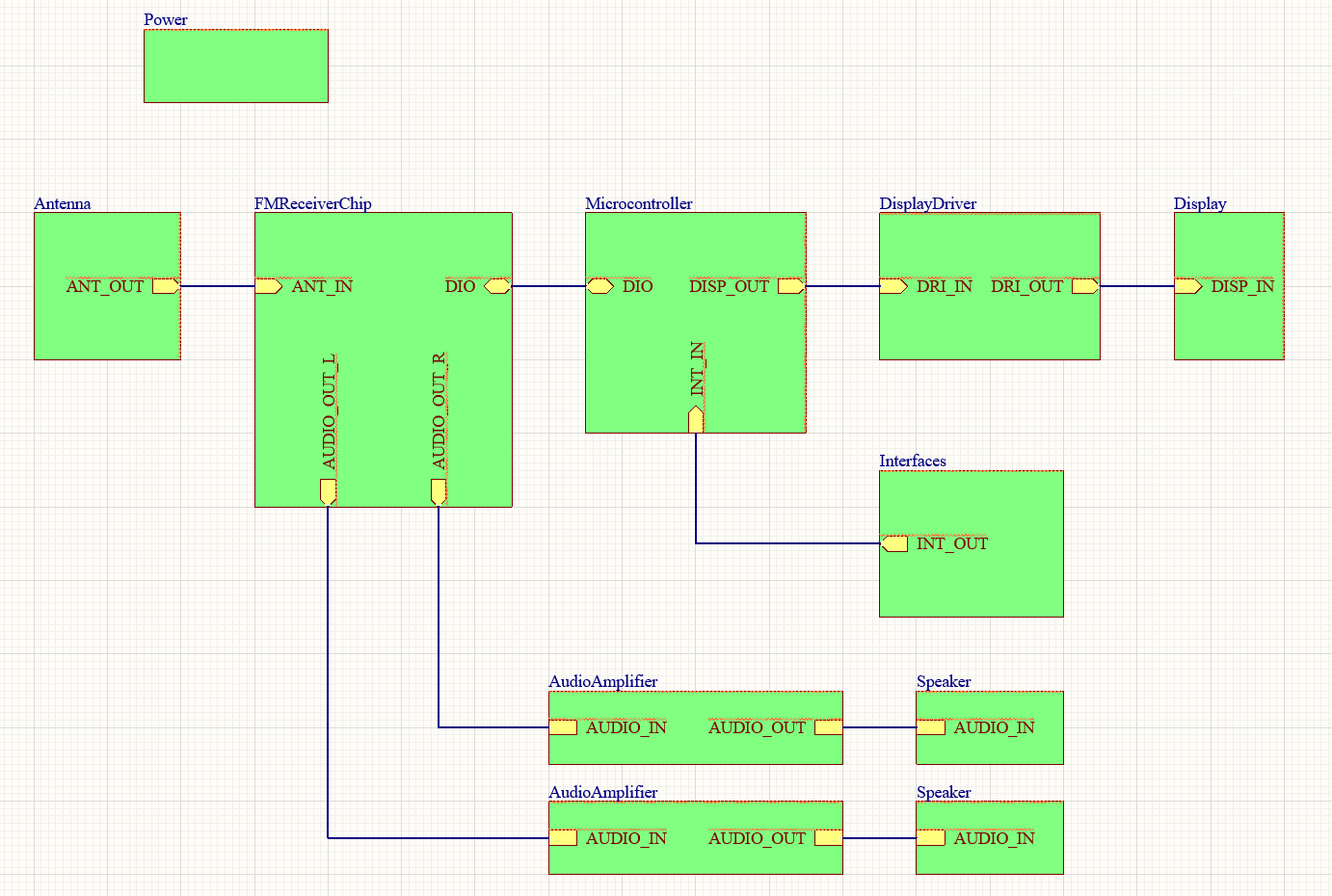
We aren’t finished with the block diagram just yet. With each block or sheet symbol, we abstract out lower-level block diagrams to simplify our schematics. We’ve done so with the antenna block, which is going to consist of have a sheet symbol within it.
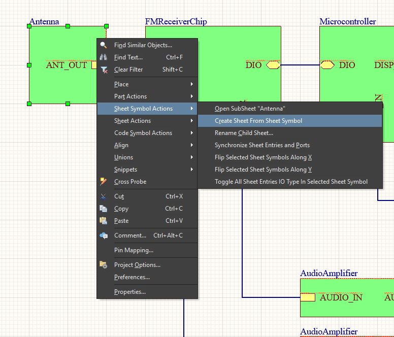
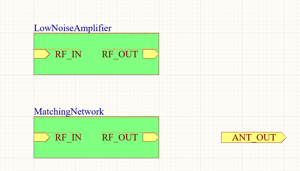
Right click on Antenna sheet symbol and select Sheet Symbol Actions->Create Sheet from Sheet Symbol. This will automatically create a new schematic sheet named Antenna.SchDoc within the project and it will add an ANT_OUT port to said schematic sheet.
Afterwards, create blocks within the Antenna schematic sheet named LowNoiseAmplifier and MatchingNetwork we won’t connect them right now, but we will need to later.
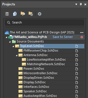
Now, let’s get all of our schematic sheets by doing selecting each sheet symbol (just as we did with the Antenna sheet symbol) and selecting Sheet Symbol Actions->Create Sheet from Sheet Symbol.
Our Projects Manager toolbar end up looking like below. Notice how sheets that present within other sheets are indented? This shows the hiearchy of the schematic sheets as provided by our top-level block diagram.
Filling in the Microcontroller
With all of our schematic sheets setup, we can begin filling them in. We’ll start small by doing a straightforward sheet: the microcontroller.
For the microcontroller, we’re using an ESP32, or more specifically the ESP32-C3-WROOM-02U-N4, which comes as module and handles a lot of the complicated supporting circuitry that’s required for a microcontroller. However! We still need to do some circuit layout ourselves for the ESP32 within the Micrcontroller sheet.
Luckily for you, we included the ESP32-C3-WROOM-02U-N4 as a component in the online Altium workspace’s library. Simply head to the Components panel on the right toolbar, and right-click the ESP32-C3-WROOM-02U-N4 to place it onto the schematic sheet.
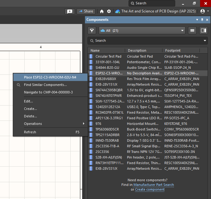
The Components panel provides all of the custom components (e.g., integrated circuits, connectors, displays) that will be needed for the FM radio.
Taking a look at the typical application circuit in the ESP32-C3-02U datasheet, draw out the schematic for the microcontroller. From the typical application circuit, you should exclude the components with the following reference designators1 and their corresponding connections:
- JP1 and JP2
- JP4
- R3
- R5
- R8 and R9
- R7
- X1
- C5 through C8
Use the following components from the Components Panel for the following reference designators found in the datasheet application circuit (note: your reference designators for these components on the Altium schematic sheet need not be the same):
| App Sch Ref Des | Component Name |
|---|---|
| JP3 | USB4085-GF-A |
| SW1 | 1437566-3 |
| R1 | 0603 10 kOhm Resistor |
| C3 | 0603 100nF Capacitor |
JP3 in particular is a USB-C receptacle, so there are some additional connections that you will need to make in addition to connecting it to the microcontroller:
- Attach a global power net to the
VBUSpins and name the global power net:VUSB. We’ll use this later to draw power from the USB-C connection - In order to control the amount of current that flows through the USB-C connection, the USB-C standard utilizes current-control resistor (CC) in order to communicate how much current a device should be provided. In the case of this FM radio, we want the maximum current that can be provided over a USB connection (about 1 A). To do so, place a shunt 5.1 kOhm resistor on each of the CC pins.
- Pins named shield/shell/mnt should always been connected to ground.
- Basic USB 2.0 communication (which is what we’ll be using to program the microcontroller) occurs over a bidirectional data line that is configured as a differential pair, which we’ll explain more about in the upcoming lectures. For now, we just need to make sure that we specify the two USB data (D) pins as a differential pair. To do so, attach a net label named
USB_D_NandUSB_D_Pto the respective sets of pins onJP3. Afterwards, attach a differential pair net label from the floating quick access menu to each of the nets. The combonation of the_Nand_Pas well as the differential pair net label, tells Altium that the USB data lines are a differential pair, which is important for later. - The 0 Ohm resistors between JP3 and the microcontroller cause an end to the differential pair net. To resolve this, name the wires on the other side of the 0 ohm resistors
USB1_D_NandUSB1_D_P, as well as also attaching another set of differential pair net labels. - Change the global power net named
VDD33in the datasheet application circuit to3.3V. We’ll need this consistency later for other devices powered by 3.3 V.

Conclusion
Congratulations on completing the first lab! You have create a full top-level schematic and began building out one of its blocks, the microcontroller.
Be sure to select Save to Server in the Projects Manager toolbar so that your work is uploaded to the course’s Altium workspace! Please do so by midnight so that course staff can grade your work.
-
The reference designator is the letter-number combination above a part on the schematic. They appear on the schematic, on the PCB itself, and in the bill-of-materials. This makes it really easy to identify components in a PCB. Each component should have a unique designator. Typical letters include: “C” stands for “capacitor”, “D” stands for “diode”, “L” is for “inductor”, “R” is for “resistor”, “P” is a connector of some sort, and “U” is a surface mount chip. Typical examples will be
U1orR4andR14. ↩
