Overview
In electronic basics (e.g., 6.200 and 2.678), you learn about lumped circuit theory and how we can represent components as ideal “lumped” models of themselves. For most electronic devices, this model works well and you can use components and route traces on a PCB as if they were their ideal representations.
However, as our circuits begin operating at greater and greater frequencies and our devices become more and more sensitive, the non-ideal natures of circuit elements begin to matter and can affect our circuits in a measurable way. In lecture 02 we delved into how we can account for these effects in our components and we can do so by representing our components in their extended lumped element models. These extended “real” models often will depend on the component’s physical packaging and our application of the device.
For example, a capacitor can be representated as the following, the middle model being the most accurate.
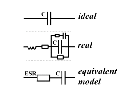 Image Credit: Commercially Available Capacitors at Cryogenic Temperatures
In this lecture, we will go over how these parasitic effects, nonidealities, and external fields can affect signals in our PCB. In understanding this, we will see how we can mitigate these effects using clever design techniques.
- What do we mean by high frequency signals
- electrical length
- Propagation through air
- Effect of noise or signal disturbances
- Example using digital signals
- Example in frequency domain (phase noise)
- Causes of signal integrity loss
- Coupling between components
- Impedance mismatch
- Lack of material control
- Lack of shielding
- Sharp discontinuities
-
Capture of external fields
- PCB emission tests (FCC)
High-Frequency Signals
High frequency signals are waveforms that change over time at a really fast rate, examples include digital communications and radio signals. What is important is that these signals have a periodic nature to them and can therefore be quantified with a
- a single or set of frequencies,
- magnitude, and
- phase,
which we can model as the superposition of multiple sinusoidal waves to help with our designing.
As the center frequency $f$ of our signal increases, its wavelength $\lambda=\frac{c}{f}$ decreases (where $c$ is the speed of light). As the wavelength approaches the length of devices and wires within our circuit, we start to experience wave phenomenon and signal integrity issues that we will need to take into account when handling our signals.
Wires can begin to act as antennas and allow energy to radiate out into the air. And the converse is also true, these wires will also be more efficent in accepting outside radiation.
Additionally, parasitic elements within our components has a greater effect on signals as their frequency increases, resulting in further non-ideal performance.
The result of this is circuits not performing as we expect and unintentional interference of other device’s functions. There are many regulations that govern the latter and the former is obviously something we do not want.
Impedance matching
The primary factor in our PCB that one needs to focus on as frequencies increase is that of the impedances present throughout our circuits.
Impedance describes how signals are effect by various circuit elements. All we really need to know when it comes to designing our PCBs is whether or not we are maintaining a constant impedance throughout our circuits and PCB.
Differences in impedance, whether it be between a transmitting device and a wire/trace or from a trace to a receiving device will result cause reflections and attenuation of any signals that pass throughout it.
 Image Credit: Wikipedia
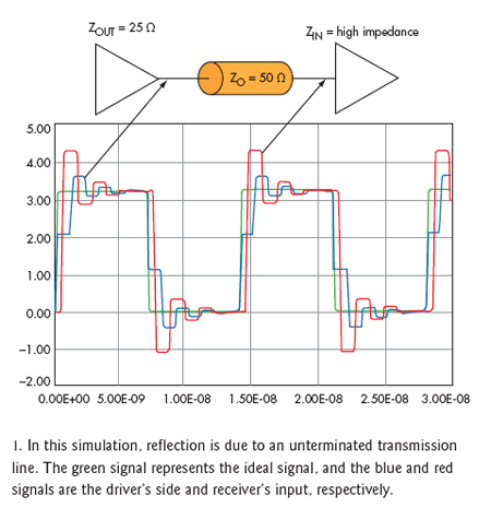 Image Credit: Electronics Stack Exchange
Components designed to handle high-frequencies (particularly in the form of ICs) will come with ports that are matched to a particular impedance (typically 50 Ohms). Therefore, as PCB designers, we have the primary responsibility of ensuring that traces and footprints match the impedance of every device. This lecture will reference impedance matching to 50 Ohms since it is the most common, but everything discussed can be applied to circuits that have different impedances.
High-frequency PCB Structures
Footprints that match 50 Ohms when soldered to a device are typically defined in a component’s datasheet. Creating 50 Ohm interconnects between devices on a board requires careful design on our side based on the PCB’s makeup and it requires we use particular high-frequency structures.
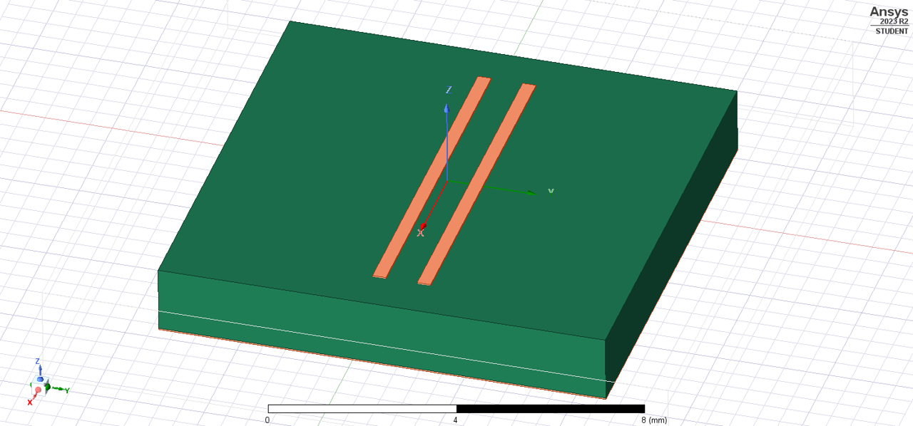
In this lecture we will focus on the microstrip structure, which is a very common PCB element that is used to carry high-frequency signals at a particular design impedance. It consists simply of a:
- Copper trace,
- Dielectric layer
- Copper ground plane
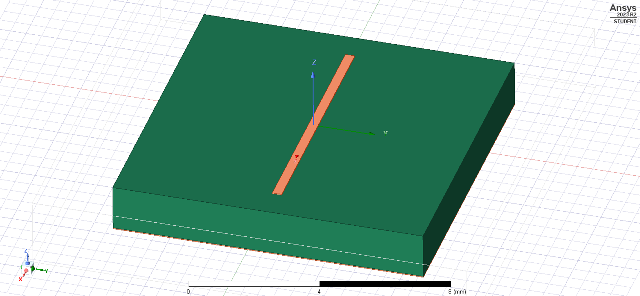
This likely describes most our the traces you would already find on a PCB, however, in order to turn a trace into a high-frequency carrying microstrip, we need to design it to have a 50 Ohm impedance. There do exist other high-frequency PCB structures that can be configured to a particular impedance such as:
- Stripline
- Coplanar Waveguide
- Substrate Integrated Waveguide
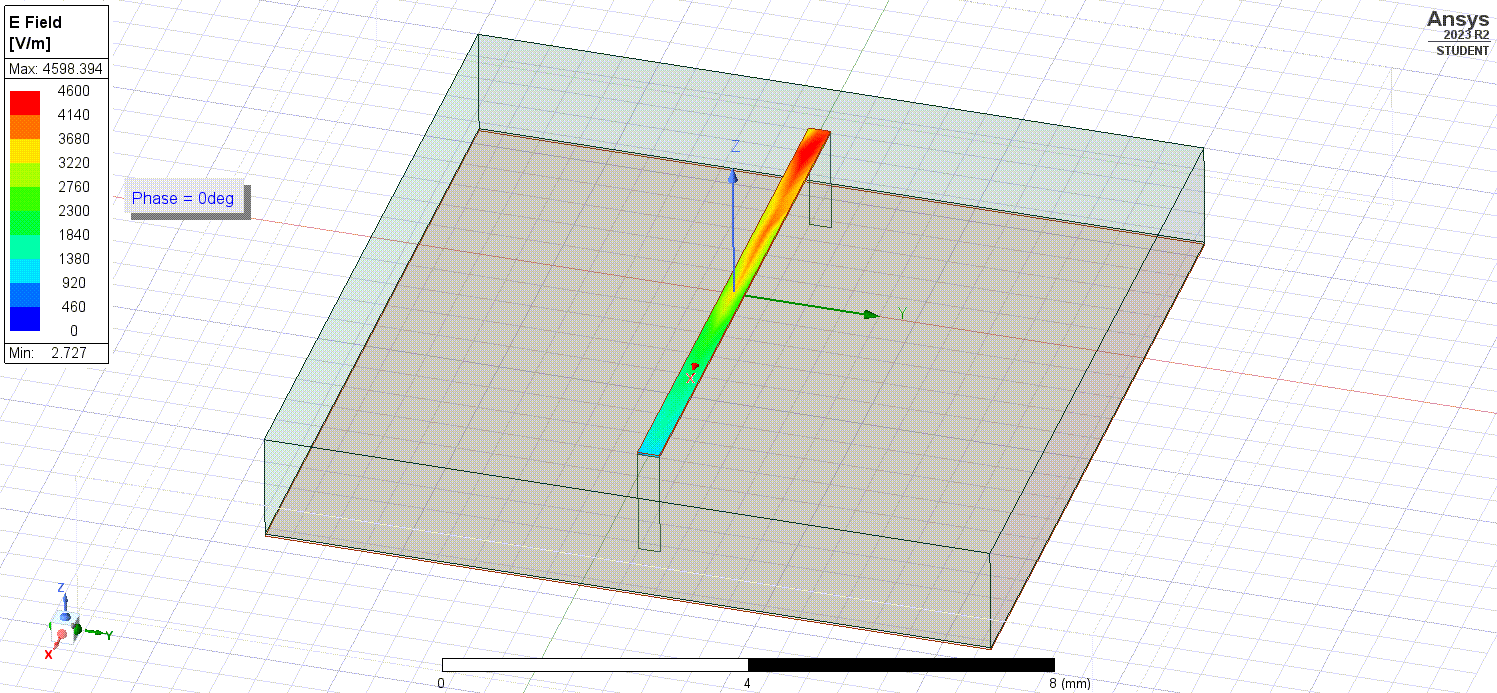
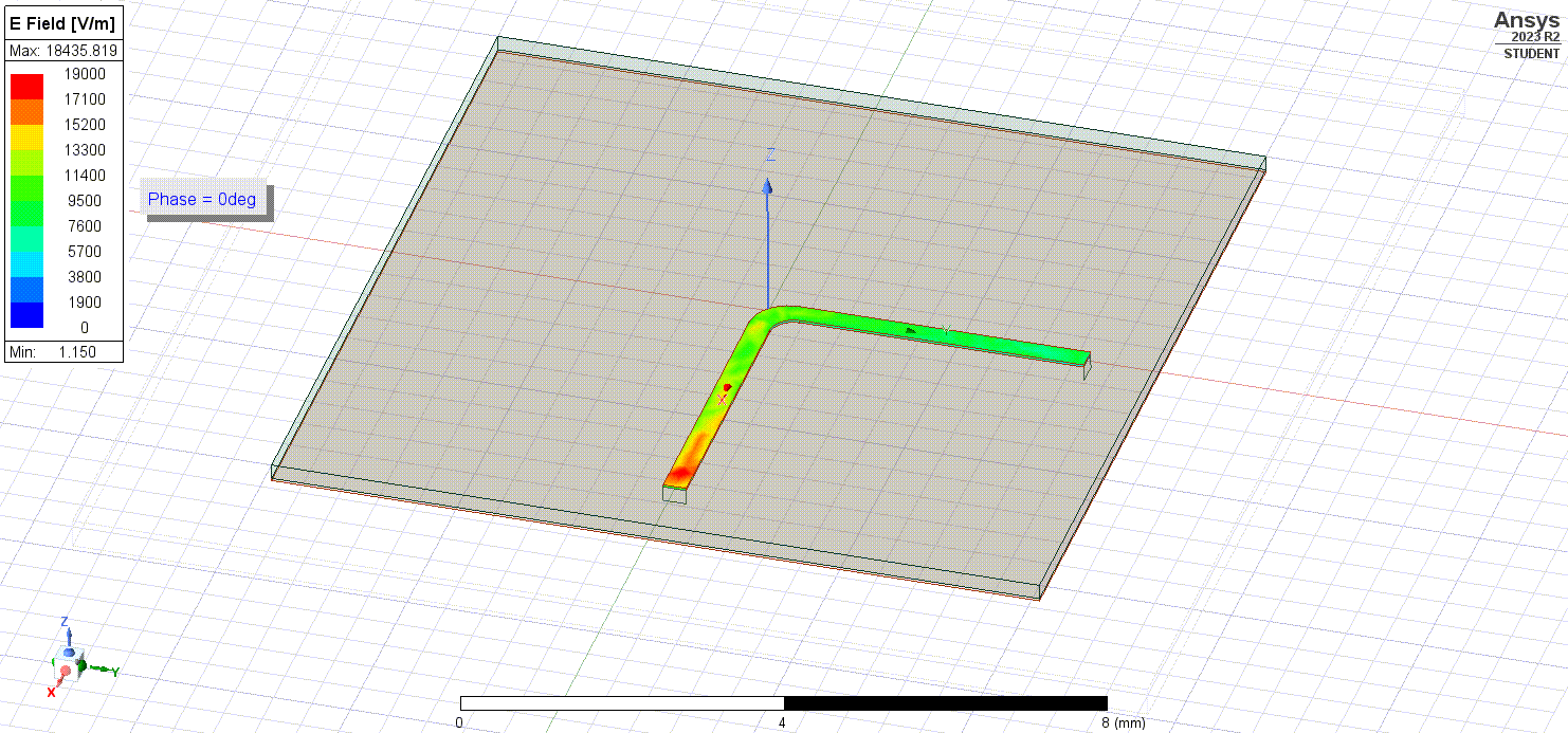
To show how microstrips perform while carrying signals, we have created an Ansys HFSS simulation with a microstrip 3D model. While not shown, either end of the microstrip model has a port attached to it which can send or receive a high-frequency waveform. For the following simulations, the signals will range from 0 to 2.4 GHz (zero being an unchanging DC voltage) coming from the port at the top of microstrip and terminating at the bottom of the microstrip.
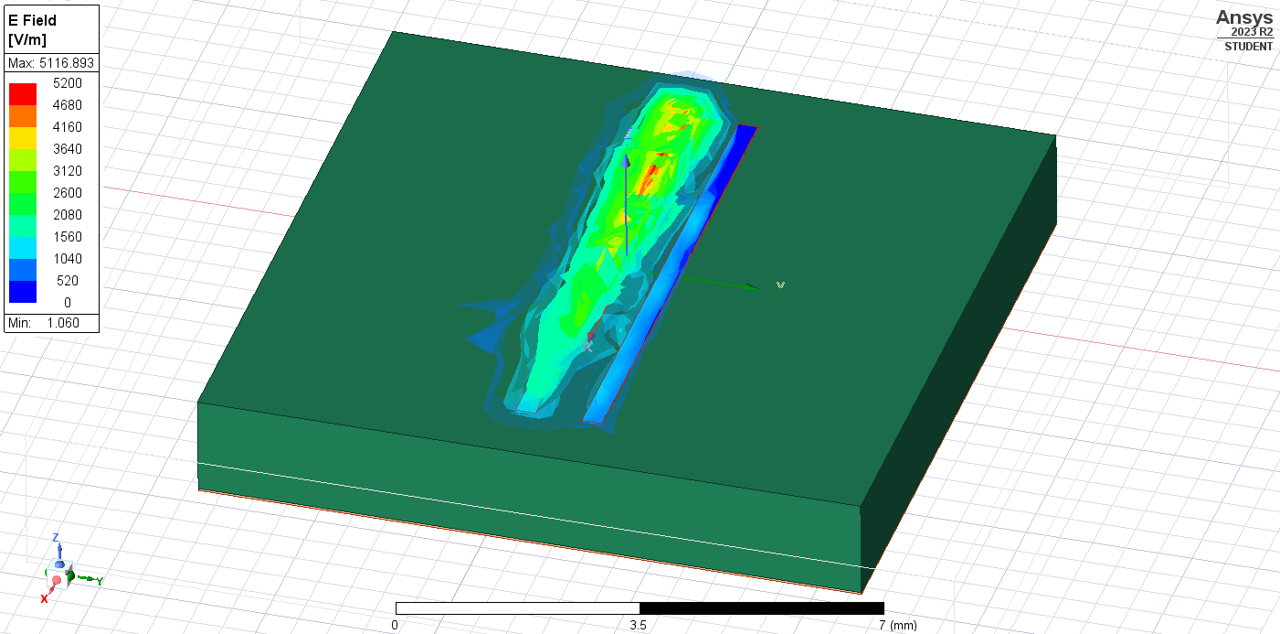
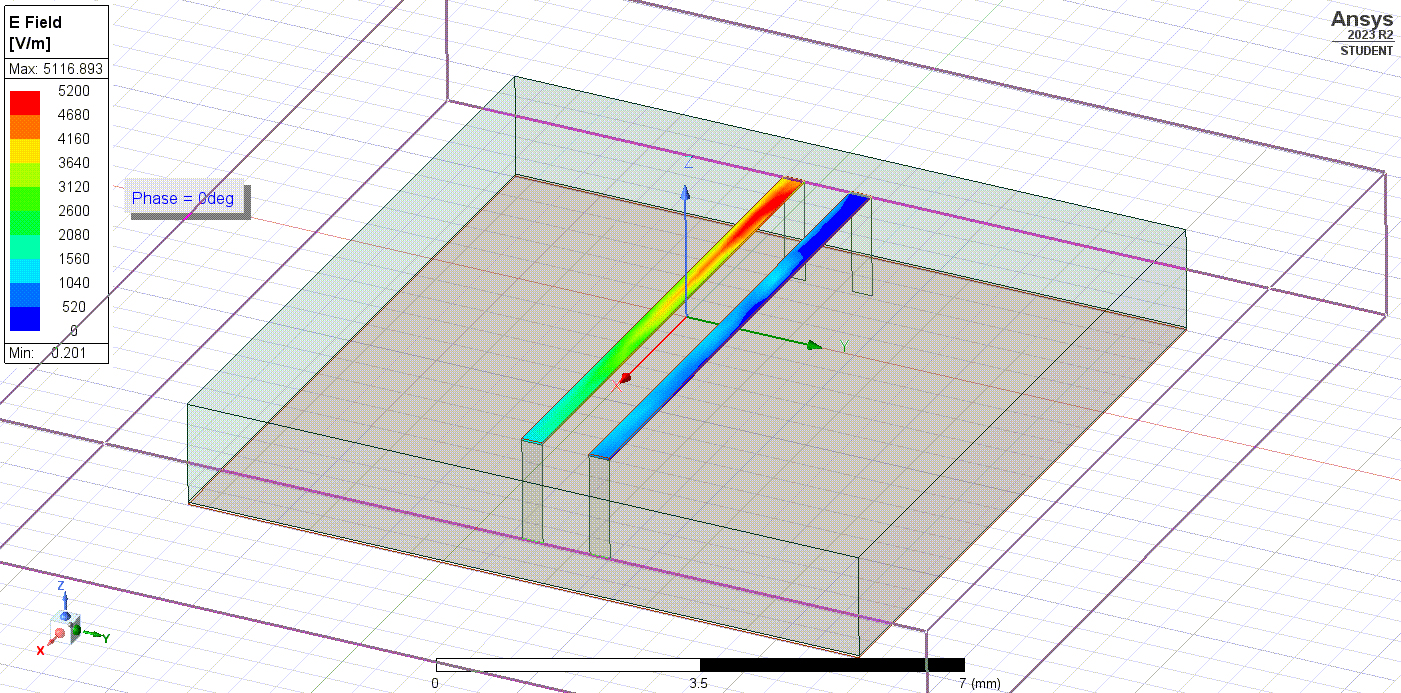
Using simulations, we can do things such as showing the electric fields flowing inside the microstrip.
As well as the electric fields outside the microstrip in the surrounding air.
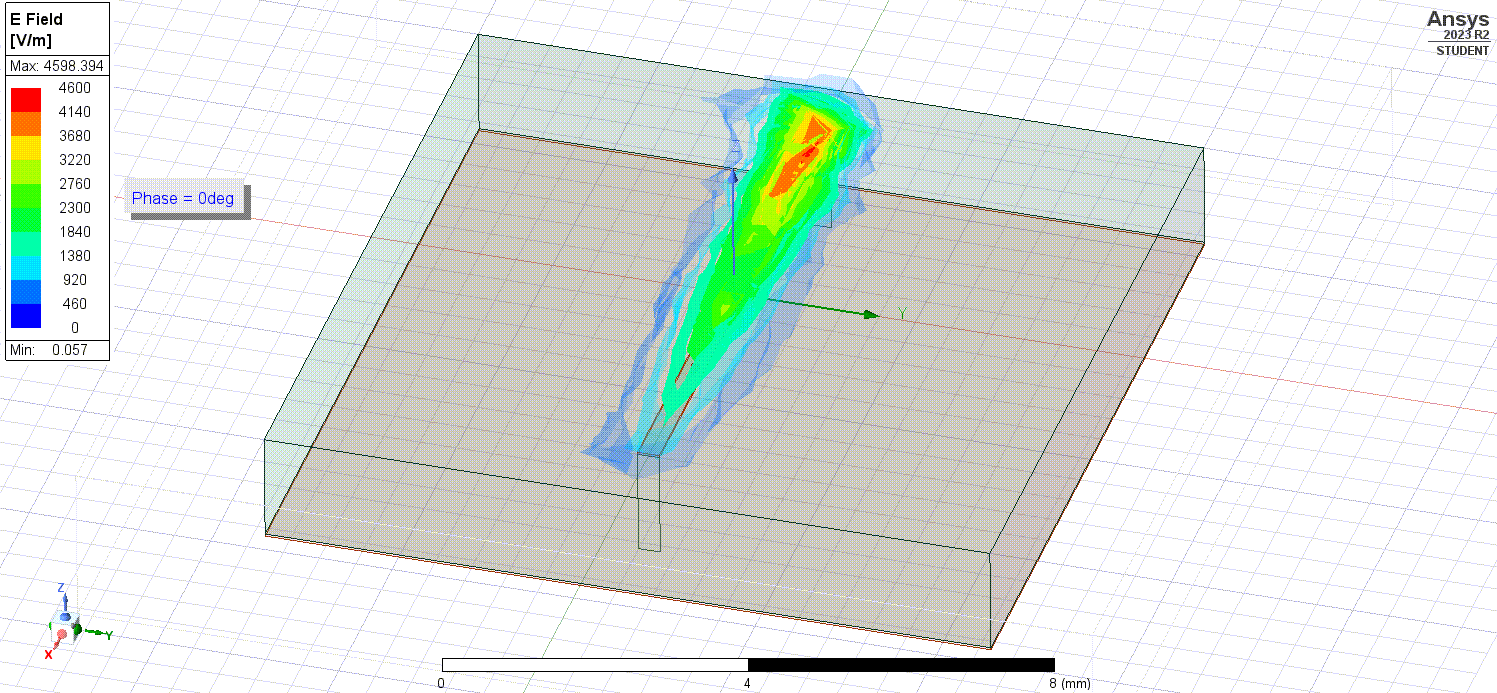
Since the microstrip is of uniform conductance/resistivity and we are visualizing it at sinusoidal steady-state (as in a while after we initially apply the signals or long after transient effects have passed), the electric fields seen are directly proportional to the currents following through the microstrip. The changing phase seen (used to animate the electric fields) is analagous to the flow of time.
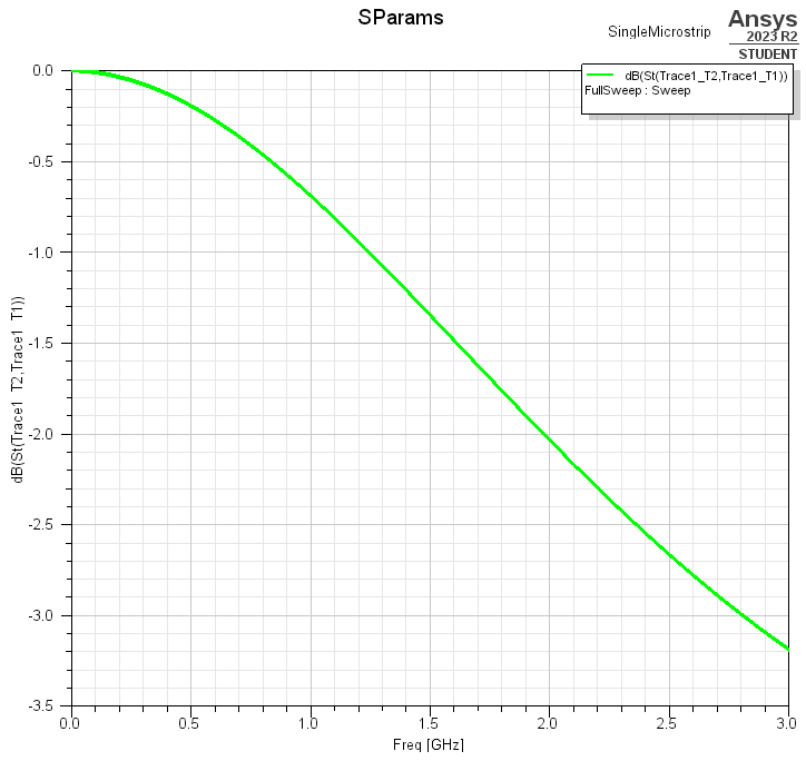
The electric field visualizations from before show the flow of a 2.4 GHz signal through our microstrip. To obtain a more quantitative analysis of how our microstrip operates under high frequencies, we can apply a sweep of different frequencies and measure the ratio between the signal power we inject at the input $P_{in}$ and the signal power we receive at the output $P_{out}$. We will measure this ratio logarithmically and call it, $10\log_{10}(\frac{P_{in}}{P_{out}})$, the insertion loss of the microstrip - measured in decibels (dB). Insertion loss measures the amount of power lost to a device, where 0 dB is no power lost and increasingly negative dB refers to greater and greater power loss.
Plotting out the sweep as insertion loss vs. input signal frequency, we see that as frequency increases, the amount of power lossed increases as well. In fact, at around 2.8 GHz we see that the insertion loss is at -3 dB, which means at that frequency about half of all the power put into the microstrip is lost!
As we will find out soon, this awful frequency response is due to the fact that the microstrip has an egregiously different impedance from 50 Ohms, and it is causing energy to radiate and reflect out of the microstrip. A well matched microstrip would typically have its curve right about on 0 dB.
If we keep the microstrip nice and uniform throughout its length, it will maintain a constant impedance throughout. This characteristic impedance is defined by multiple factors in the microstrip’s design, which include:
- Substrate height
- Substrate dielectric constant (Dk, $\epsilon_r$,)
- Trace/copper thickness
- Trace width
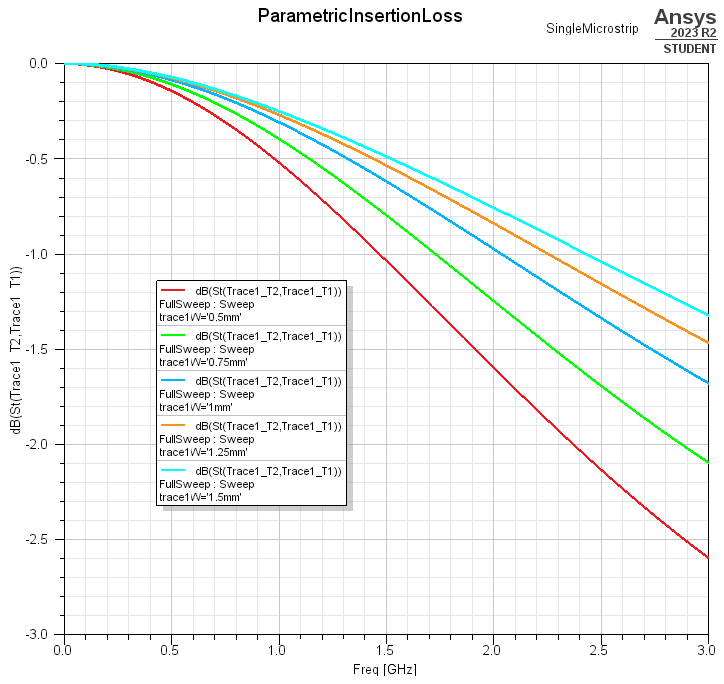
Often times, the only thing factor we can granularly change on our own is the trace width, so it becomes our primary tool for adjusting the impedance of our microstrip. The other three factors are typically set by the board fabricator and often will require additional cost in order to change
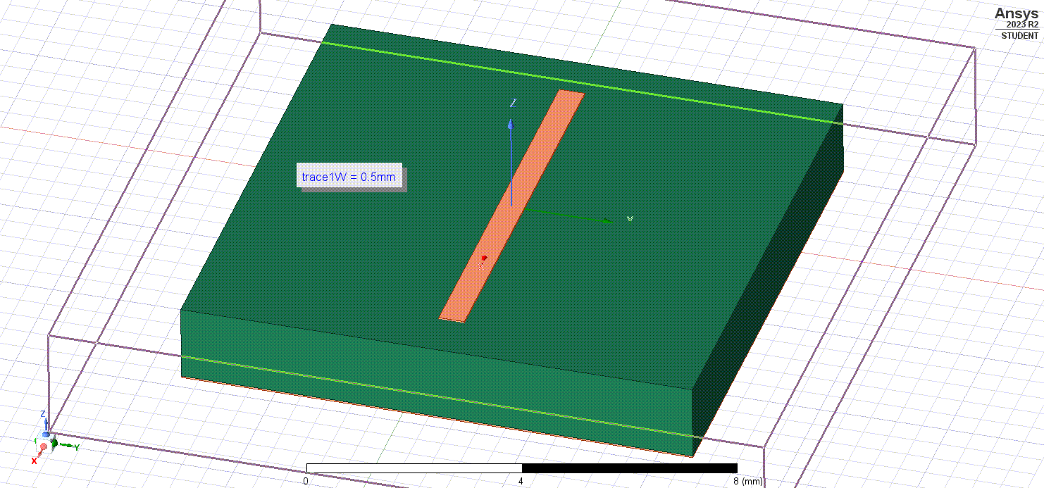
We should be able to change the impedance of the microstrip by changing its width. There exists formulas and calculators that can be used to determine the theoretical impedance of a microstrip. Our microstrip with its current parameters comes out to and impedance of ~121 Ohms - quite a lot greater than the 50 Ohms of our ports and is definitely the reason for the huge losses we have been seeing.
Widening the trace should lower its impedance, and therefore improve its signal carrying abilities. We can see that in the plot below, our insertion loss curve shifts closer and closer towards 0 dB as we increase our trace width!
One thing to notice, however, is that at the best insertion loss performance the microstrip is already 1.5 mm wide, and that is quite large! By the time we reach an impedance of 50 Ohms, the microstrip will probably be too large for our board and we will start to get problems interfacing from the port of an IC and the microstrip. This issue gets back to the point on how PCB designers will often have to adjust other factors about our PCB stackup (and spend extra cash) in order to ensure high-frequency structures maintain reasonable dimensions.
Coupling
Now that we know how microstrip performs on a bare PCB, it would be a good idea to understand how it acts in the prescence of other microstrips, such as traces routed in parallel. We can as always model this out.
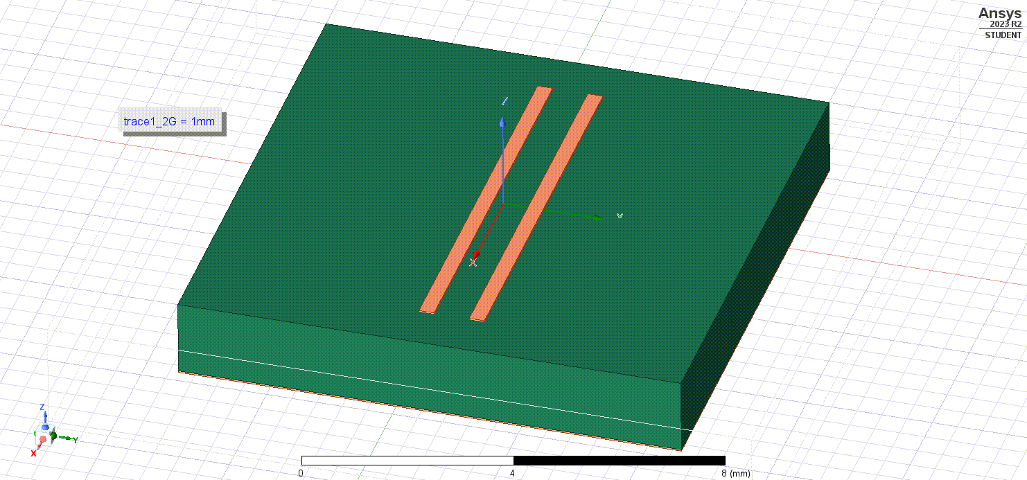
Below, we have two identical microstrips placed right next to another. only the leftmost trace will receive any signals for the following simulations and the rightmost trace will simply remained terminated to 50 Ohms on either end.
When we simulate out the electric fields in the surrounding air, we can notice something quite interesting: the electric fields from the leftmost microstrip are reaching the rightmost microstrip!
These electric fields in the air are clearly inducing electric fields within the nondriven conductor. To show that this is really the case and not a visual artifact, we can plot the electric fields within the conductors only. There, we can see that there is a changing electric field being created from the coupling of one trace to the other, and (minus some degredation in amplitude and phase) both signals in either conductor are the same.
Coupling between high-frequency traces is an inherent phenomenon of near-field radiation, and it is exacerbated by an increases in frequency. If we plot the ratio of power between the left and right microstrips, and call it the coupling factor, we can see that as we increase frequency, coupling factor increases. A coupling factor of 0 dB would entail that the full amount of power that is sent through one trace is completely coupled to the other trace with zero loss.
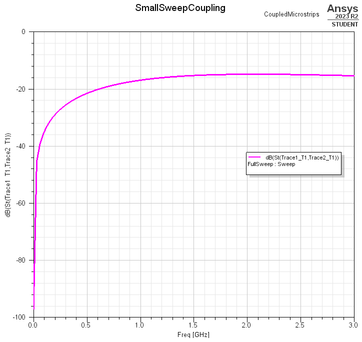
Signal coupling can become a huge issue, primarily from the interference it introduces between traces. If the coupling factor is great enough and signals are sent at high-enough powers, a trace can couple its signal to another trace and create false signals (i.e., we experience similar issues as to if we made an electrical shorts between seperate traces).
So how do we mitigate this problem? One of the simpler and more obvious answers is to increase the distance between our coupling traces. The radiation emanating from one parallel conductor to another is amproximately inverse-squared proportional to the distance between them.
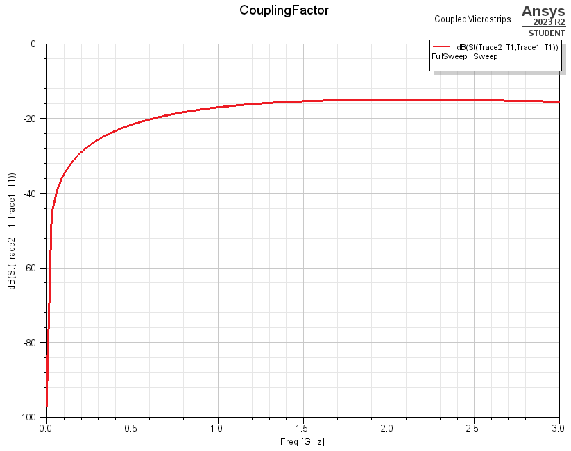
Plotting the frequency response out for each particular trace gap distance, we notice that the coupling factor significantly decreases with increasing separation.
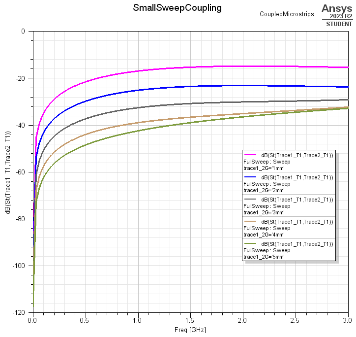
This is great to see, but on a space-constrained board it is simply not feasible to put large gaps between traces to reduce coupling.
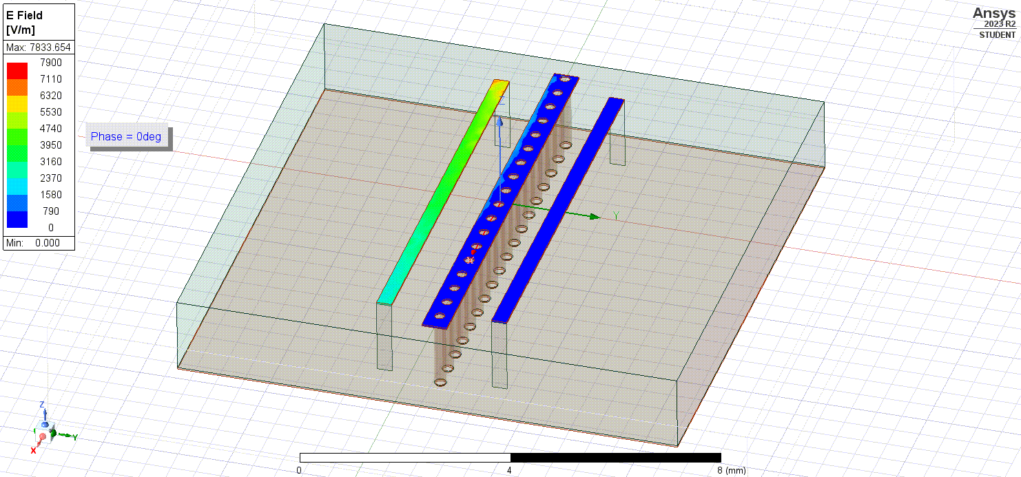
What if then, instead of trying to avoid the radiating coupling fields we instead shielded against them? One way we could do this is to create a copper pour/trace between our microstrips that is connected to ground. We can also try adding via stitches as well to create a better shield and lower impedance path to ground.
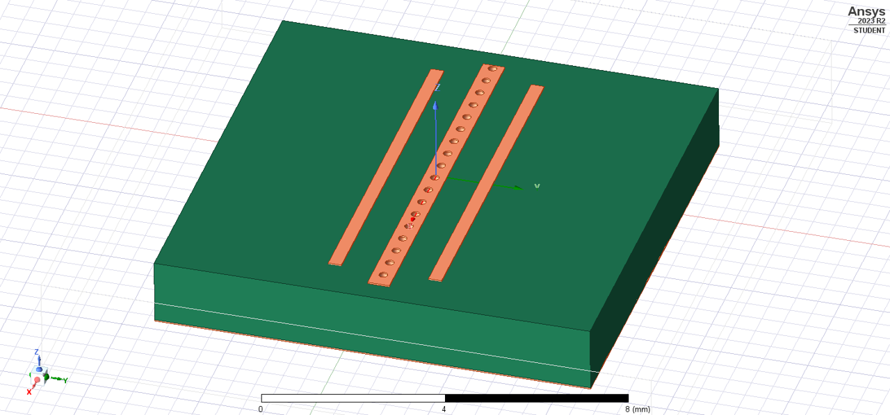
Now if we simulate the electric fields flowing within our conductors, we notice that they exit the rightmost (excited) trace and couple to the ground pour instead of the leftmost trace!
Taking a look at the coupling factor,
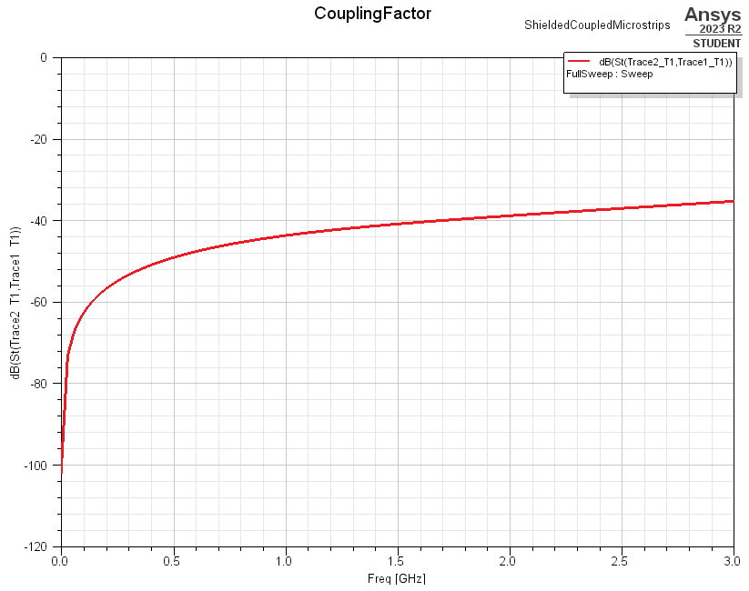
Comparing that to the unshielded microstrips at the same distance (2 mm) from each other,
And we can notice a 20 dB reduction in coupling between the two traces - that is a 100 times improvement!
Ultimately, what this shows is that ground pours, planes, and via stitching provide a significant reduction in the coupling that occurs between traces as well as interference that could be coming externally to our PCB. And the great thing about them is that we can easily add ground pours and via stitching to our high-frequency PCB layouts.
Discontinuities
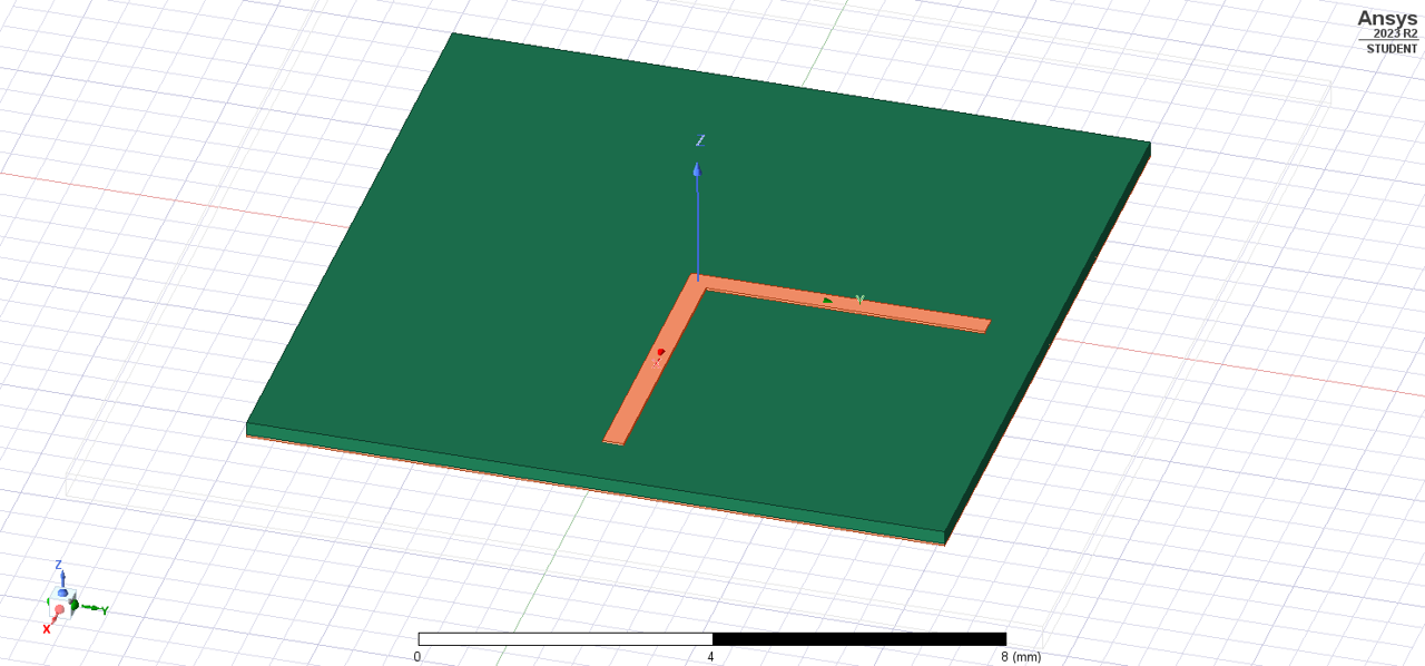
We discussed initially that changes in the physical structure of traces and materials can result in impedance changes, and impedance changes can lead to radiation of electromagnetic fields. This is particularly the case when we have to make any bends in our high-frequency traces. The bend itself disrupts the uniformity of the microstrip and can lead to impedance mismatch from its own resonation.
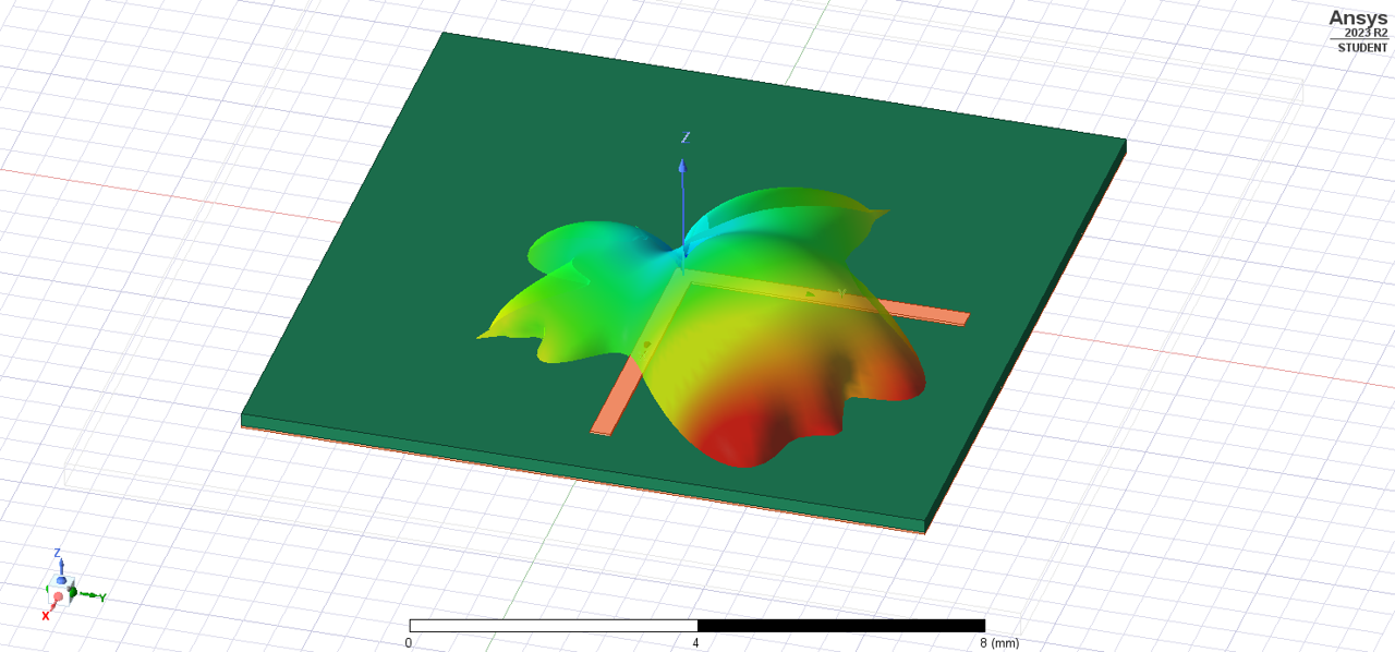
One egregious example is a sharp, 90-degree bend.
When we plot the electric fields flowing through the bent traces, we notice that they lack some uniformity due to the discontinuity.

It causes greater signal loss through the bend as well as sharp, powerful radiated fields that could potentially interfere with devices located nearby.
Our solution? Smooth, wide bends reduce the change in impedance.

And this reduced discontinuity we can see through the more uniformly distributed electric fields.
Finally, looking at the near-field radiation pattern, a rounder, weaker beam is the result (although there are no legends/scales, the red region in the smooth bend is of lower radiative intensity compared to the same red regions in the 90 degree bend).
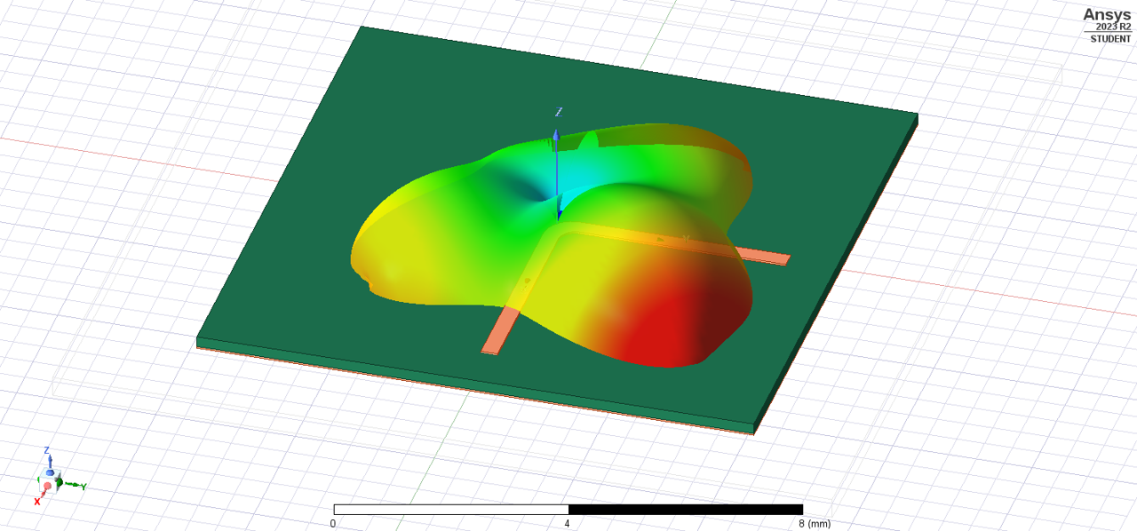
The takeaway from this analysis is that we wish to utilize smooth, wide (or ideally, zero) bends in our high-frequency microstrips to reduce impedance mistmatches caused by discontinuities and unintended signal radiation.
Examples
28 GHz Amplifier
Notice the:
- Straight, unbent and short traces
- Copper ground pour throughout (with a metal block soldered underneath to further lower return path impedance)
- Use of coplanar-waveguide high-frequency transmission line structure (an alternative to microstrips)
- Connectors, device (amplifier), and traces are each matched to 50 Ohms
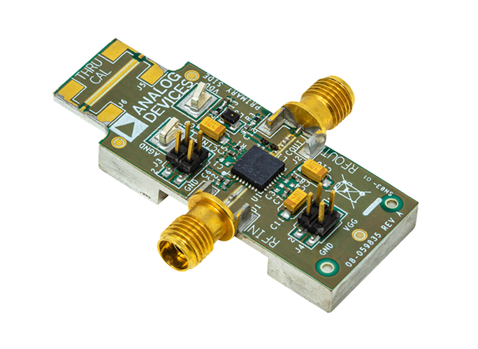 Image Credit: Analog Devices
24 GHz Radar
Notice the:
- Straight, smoothly bent traces
- Copper ground pour throughout (with multiple ground planes located on internal laters)
- Use of coplanar-waveguide high-frequency transmission line structure (an alternative to microstrips)
- Connectors, devices, and traces are each matched to 50 Ohms
- Relatively wide distaces put between high-frequency RF traces
- Vias (which connect to the phased array antenna on the bottom of the board) are carefully sized to maintain a 50 Ohm impedance.
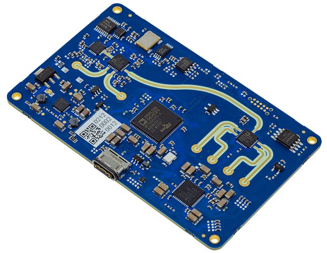 Image Credit: Analog Devices