Overview
Last lecture, we delved into the basics of layout as well as the technologies used to create a working PCB. In this lecture, we will survey the considerations a designer must take when designing any kind of PCB.
Background
Maxwell’s equations
Given Maxwell’s equations in steady-state conduction:
- $\vec{\nabla} \cdot \vec{E} = \frac{\rho}{\epsilon}$ - Describes how charges produce electric fields
- $\vec{\nabla} \cdot \vec{H} = 0$ - Describes how magnetic field lines never end
- $\vec{\nabla} \times \vec{E} = -\mu \frac{\partial{\vec{H}}}{\partial{t}}$ - Describes how a changing magnetic field will induce an electric field
- $\vec{\nabla} \times \vec{H} = \epsilon \frac{\partial{\vec{E}}}{\partial{t}}+\sigma\vec{E}$ - Describes how bulk and changing electric fields induce magnetic fields
We can also derive the following:
- $V = -\int \vec{E} \cdot d\vec{c} = \frac{\partial\lambda}{\partial t}$ - A potential is created through a change in magnetic linked flux
- $\vec{J} = \sigma \vec{E} \rightarrow I = \sigma\iint \vec{E} \cdot d\vec{s}$ - A current is induced by an electric flux within conductive materials
- $I = \frac{\lambda}{L}$ - A current is induced by a linked magnetic flux (proportional to inductance, $L$)
What these equations show is that both external magnetic and electric fields have the capability to induce unwanted voltages and currents within our circuits. While in the presence of fields that are emitted by normal electronic devices, these voltages and currents will be tiny, they can have a large effect on sensitive analog signals and high-frequency components.
One fun way to test out this phenomenon can be done by taking a multimeter (or even an oscilloscope) and placing it into a low (milliVolt) AC voltage measurement setting. If you spread out the multimeter leads you might notice that the voltage reading increases by a tiny bit as you create a dipole antenna that captures radiated (far-field) electromagnetic signals. If you then take one of the leads and closely place it parallel to a mains power cable, the AC voltage reading will increase significantly as (near-field) coupling occurs between the cable and the multimeter.
Therefore, in PCBs involving any sort of high-frequency or sensitive componentry, we need to employ methods and design techniques that minimize our board’s susceptibility to external electromagnetic radiation in order to preserve the correct function of our circuits.
Electrical design concerns
- Stray charges and external fields can induce unwanted signals and noise in our circuits
- As the operating frequency of our circuits increase and the size of them decreases, they become more sensitive to noise.
- Imperfect conductors (any material that is not a superconductor) contains resistance that can generate heat under high currents and cause voltage gradients
- Imperfect insulators (any material that is not pure vaccum) can cause parasitic effects.
This lecture will primarily go over how we mitigate these concerns in the PCB layout process
Routing and Placement Considerations
Minimizing trace resistance
Recall that every imperfect conductor contains its own inherent material resistivity, $\rho$, and we can calculate the bulk resistance of a piece of conductor using $R = \frac{\rho L}{A}$, where $A$ is the cross section of the conductor.
This characteristic implies that since we can not change the conductive material we use on a PCB (it is always going to be copper), then the only way we can control the bulk resistance of a trace is by adjusting its length and width (the height/thickness of a trace is usually set throughout the PCB, referred often to as the copper weight by the fabricator).
As current passes through resistive material, energy is lost and emitted at heat. Therefore, to minimize electrical losses and to reduce the heat emitted from a trace in high current applications, use wide trace widths and keep connections short.
- In general, ensure traces are wide enough so that the temperature rise as a result of current flowing through the trace stays below 10 degrees Celcius.
- Polygon Pours can help in designing wide traces, particularly for high current nets
- 10 mil (0.254 mm) wide traces are generally fine for up to 1A of current
- For very high current traces, its soldermask can be removed so that solder can be added on top during assembly to increase its effective cross section
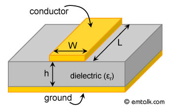 Image credit: em: talk
High-frequency signals will often require impedance matched traces in order to avoid transmission distortions. On a PCB, this will typically consist of planar microwave structures such as microstrips or coplanar waveguides. Such structures will have precise trace width and clearance constraints that depend on the board stackup.
- For traces requiring a particular characteristic impedance, use your PCB EDA software as well as your board stackup to calculate the required trace widths and routing requirements
- Avoid sharp turns with high frequency traces, use smooth bends only. Sharp discontinuities will result in impedance distortion and unwanted radiation
- Removing soldermask from impedance-matched traces will prevent distortions caused by the soldermask’s dielectric properties
Reducing capture of external electromagnetic radiation
External fields captured by our circuits will convert into noise-y voltages that can adversely effect signals within our PCB. Minimizing the amount of fields captured can improve the performance of high-frequency or wireless functions of our PCB design.
Conversely, design techniques that reduce susceptibility to external radiation will also reduce the amount of radiation that the board emits on its own. This can help with avoiding self-interference and for meeting regulatory emissions guidelines
Excessively long traces can form loops that can capture external magnetic fields and antennas that can absorb electromagnetic radiation.
- Keep traces as short as possible
Sharp corners in traces carrying high-frequency signals will lead to impedance changes and can act as radiators
- For high-frequency traces, use smooth bends and avoid sharp 90-degree turns
Ground planes can help shield external fields and will provide a low impedance return path for high-frequency devices.
- Use ground planes generously.
- Fill empty spaces on signal layers with ground pours
- When there are multiple ground planes or pours, using via stitching to connect them together
To further shield sensitive components, physical metal shielding can be added on the outside layers.
- Shields require a generous connection to ground
- Metal shields are good at protecting from external electric fields
- Highly permeable materials (e.g., steel and iron) are needed to protect from external magnetic fields
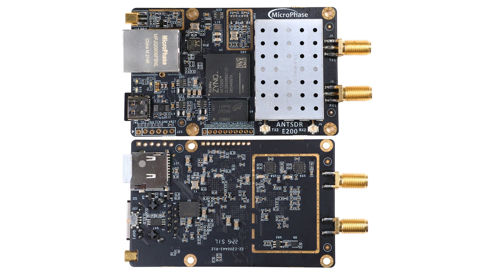 Image credit: AntSDR
Edge effects consist of the fringing fields formed by unintended inductive loops and capacitors inherent to a PCB. These fringing fields can not only be emitted and interfere with nearby devices but also act as capture points of external fields.
- Follow the 10h rule: high frequency planes and traces should be routed at least a distance ten times the height of substrate layer from the board edge to avoid the edge fringing effects.
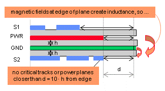 Image credit: EMC Standards
Minimizing effects of electrical noise
However, sometimes when there are multiple high-frequency circuits (e.g., digital and analog sections) that share the same PCB but occupy different sections of the board, split ground planes can be used to isolate the noise generated by each of the circuits to within their own areas.
- This primiarily concerns the internal ground planes
- Cutouts in the ground plane can be made on the border between two circuit sections on a board to create split (but still connected) ground
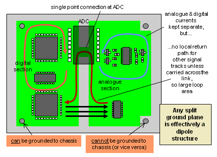 Image credit: EMC Standards
Similar to ground planes, internal layers can also be divied up into power planes which consist of copper pours dedicated to a single power net. This isolates noise from each power net and allows for easier routing
- Vias are used to connect components on the outside layers to the power nets
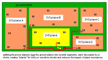 Image credit: EMC Standards
Decoupling ICs, as discussed many times before, involves placing capacitors near ICs attached from the power nets to ground in order to filter out high-frequency noise and protect from voltage transients.
- Multiple capacitors of different values can be used in parrallel to form broadband noise filters
- The closer to the IC the decoupling capacitors are, the better.
- Decoupling capacitors need a good, short connection to ground
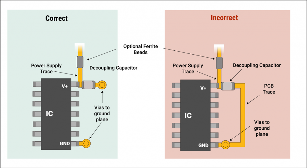 Image credit: Sierra Circuits
Coupling can occur through neighboring traces in which signals within one trace are induced in the neighboring trace. This can cause self-interference within the board (known as crosstalk).
- Follow the 3w rule: neighboring signal traces should be at least three trace widths apart in order to avoid crosstalk
- Ground pours can act as shielding between traces
- In general, keep noisy traces (typically ones assigned to power nets) away from sensitive high-frequency traces to avoid noise coupling. High-frequency traces also need to be kept away from each other
In the extreme case, traces that are carrying high voltages (>24 volts) can experience arcing via dielectric breakdown if traces and planes are not made far enough apart.
- Ensure that traces are far enough apart as to avoid any arcing based off more than double of voltage the trace intended to be
- Verify that the substrate and its thickness is appropriate for the voltage levels you will be using as arcing can occur through the board itself
Mechanical and manufacturability considerations
Trace spacing and general clearance requirements are often specified by a board manufacturer to denote their fabrication capabilities. It is important to follow these guidelines to ensure that the board is manufactured correctly, especially when it comes to traces clearances
- Too close of traces can end up being fabricated as a single trace or with shorts
- Ensure the board fabricator’s manufacturing minimums are met, then apply trace width guidelines for current or impedance matching
Integrated Circuits (IC) tend to produce a significant amount of heat during operation, which must be continuously removed to avoid overheating and ensure the IC’s correct operation. As a result, most ICs contain thermal pads underneath which must be soldered to during assembly and are part of the ground net. Adding thermal vias can further help wick away heat and improve the ground connection to the chip.
- Often an IC’s footprint will not come with thermal vias, be sure to add them to the board or to the footprint
- The size of the via hole will determine whether or not solder ends up being wicked through it
- A larger filled via (with solder) will have a margninally better current conductivity and thermal conductivity, but may lead to voiding where the chip’s thermal pad does not have enough solder to bind it properly to the board
- Smaller vias will not be able to wick solder
In order to improve solderability, thermal reliefs are created around pads that are surrounded by copper pours of the same net. These thermal reliefs consist of cutouts of the copper around the pad and spokes that end up connecting the pad to the surounding copper. This method limits the amount of heat that can be wicked away from the pad during soldering while maintaining an electrical connection, which ultimately makes soldering to it easier.
- Thermal reliefs do limit the amount of connection achieved between a pad and surrounding copper and therefore should not be used in high current or high-frequency applications
A freshly designed and fabricated PCB often never works intitially as intended. Testpoints are small exposed pads on the PCB that connect to traces or device pads to allow for sampling of a particular net.
- Ensure that plenty of testpoints are placed and connected to important nets to allow for future debugging or repair
- Avoid placing test pads on impedance-controlled traces as the pad can cause distortions and impedance mismatch
A board needs connectors to allow for external interfacing. These connectors must be selected to meet the specifications of the signals or currents they will be carrying and have a proper mechanical rigidity suitable for what they will be interfacing with.
- Connectors often come in edge mount or board mount configurations. Edge mount options often are easier to interface with and implement with an enclosure
- They also will come in surface mount and through-hole options. The latter is more flexible and allows components to mounted on the opposite side of the board (or ensure a flat bottom side) but they can easily be delaminated from excessive stress. For most applications, its recommended to use through-hole mounted connector for their better structural rigidity.
Mounting holes are useful for adding an enclosure to a board
- It often does not hurt to add mounting holes to the corners of a board
- Mounting holes can be made with an exposed annular ring and assigned to the ground net to ground a metal enclosure with the board’s ground
Examples
RF/Microwave
The EVAL-HMC994APM5 by Analog Devices is an evaluation board for their 28 GHz power amplifier.
What to notice:
- Ground pour throughout the board and a metal block attached to the bottom to increase ground plane cross section
- Impedance-controlled traces between the central IC and the connectors with soldermask removed
- Traces are made as short as possible
- A “test coupon” is included to allow testing of impedance of the traces used
- Special substrate is used for its superior RF/microwave performance
- Many testpoints are included
- The connectors are appropriately selected to handle very high frequencies
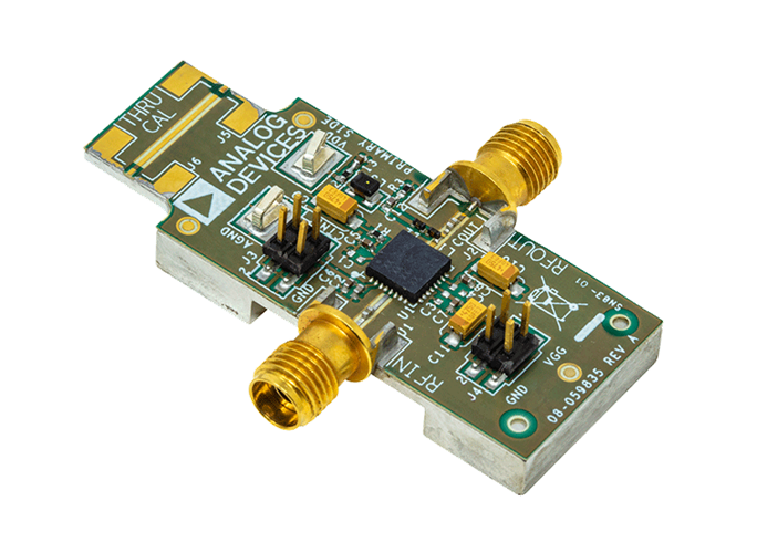 Image credit: Analog Devices
High-Speed Digital
The EVAL-AD9694 by Analog Devices is an evaluation board for their 135 MHz analog to digital converter.
What to notice:
- Ground pours throughout the board
- Impedance-controlled, differential traces for the analog sampling signals (each ADC channel is differential) with corresponding SMA connector pairs
- Far separated digital and analog sections with their own ground planes
- Many mounting holes
- Many debug and test points
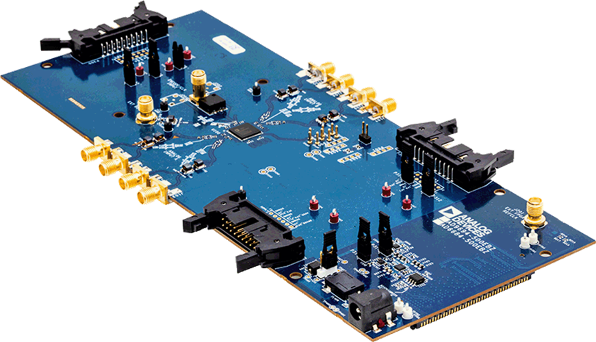 Image credit: Analog Devices
High Power
The DC2174A-B by Analog Devices is a demo board for their 70 A Dual output buck converter
What to notice:
- Wide traces are used across layers for input and output with via stitches. Copper pours are used to make them.
- Appropriate high current crimped connectors are used for the high-current output
- Additional PTH connectors are mounted along the edge
- No thermal reliefs around pads
- Mounting holes for standoffs
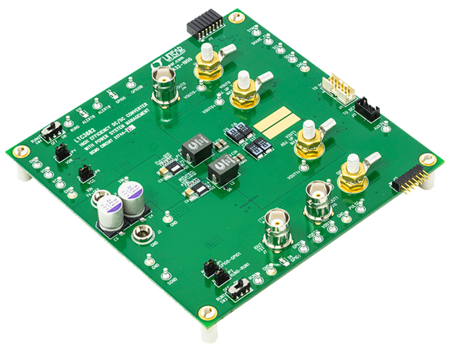 Image credit: Analog Devices