A Brief Overview of Layout
Layout is the FUN part of PCB design! And, after circuit design, it is 90% of the actual work of making a PCB. You can think of PCB layout as an “Introduction to Urban Planning for the Distinguished Electrical Engineer,” mostly because that’s EXACTLY what it is.
Your PCB is a City of Tiny Electrons
Think of your PCB as a city. The electrons are the people and they have places to go, things to do. The components are buildings where they go do their business, and the traces are the roads that take them there. Bear with this analogy for a brief amount of time to explain some basic concepts:
- Cities have zones for different types of land use, industrial districts, residential districts, the idea being to keep activities in the areas they need to be in without affecting life in other areas. PCBs are the same, we seperate the board area based on the types of use. Power goes in one spot, digital signals goes in another, and analog has its own space as well so there is no interference or overlap. (We will talk about this more below).
- The best cities have short and direct roads with relevant buildings placed near each other. People are lazy, so are electrons, and most do not like walking far distances to get where they need to go. People can get distracted and meander off-path, electrons can pick up interference that will not let them do their job as effectively. Therefore our job as PCB designers will be to place relevant components as close together as possible to minize the lenght of the traces in-between them.
What’s a PCB?
Let us start off with defining a PCB and from there we can further define layout.
A PCB is a Printed Circuit Board, and fundamentally it’s just a flat piece of material that connects electronic parts together. You’ve likely seen them before, but here’s a couple examples of what they can look like:


These are known as rigid PCBs, and they are made by taking a flat piece of nonconductive substrate, bonding conductive copper to either side, and then selectively etching away the copper to make connections between the components you want. Components mount to either the surface of the board, or they have leads that go through the board and solder to the hole.

Image Courtesy of Evil Mad Scientist Laboratories
The photo above shows a simple 2-layer rigid PCB, but there are a few other ways we can build our PCBs:
-
Multi-layer PCBs - Exactly the same thing, except taken a little further. After the copper etching is done, a thin layer of bonding dielectric called prepreg is applied to either side, and then another layer of copper is applied to that. That copper gets etched, forming another set of copper layers on the PCB. This lets you route more signals, since you can now have more space to go through/around other signals on the board. Super high layer count boards are possible - you will be making 2-layer boards for simplicity, but 12-layer boards are pretty common in super mass produced consumer electronics.
-
Aluminum/Ceramic PCBs - Which are just like a normal PCB, except the dielectric is aluminum, ceramic, or some other substrate. This is normally done if you need a PCB that’s more thermally conductive and can conduct heat away from components faster then typical dielectric (such as FR4 fiberglass) can. Aluminum can conduct better than fiberglass, ceramic can conduct better than aluminum.
-
Flex PCBs - Which use polyimide instead of a rigid dielectric substrate. Polyimide is flexible, which makes flex PCBs really good for actuators (which have moving parts, but the PCB itself is the moving part) and interconnects between boards - since the PCB is bendy, the cables that normally connect PCBs can become the PCB itself. This technology is the backbone of the iPhone, which uses them everywhere, like this:
-
Rigid-Flex PCBs - As you can probably guess, this is just a mix of the two technologies. We can laminate fiberglass and polyimide in the right order, and make something that has a rigid section, and something with a flexible section.
-
Substrate-like PCBs (SLP) - Also exists and allow for really complicated routing. This almost makes a chip-to-chip interconnect with the density of a chip.
How Do We Layout?
Location of Components
The FIRST STEP once you start your layout is placing and orienting all your components.
Typically in your PCB EDA software (e.g., Altium and KiCad) you will use rooms to help section off similar components into the same areas. In the next lecture, we will go further in-depth into how ideal component placements.
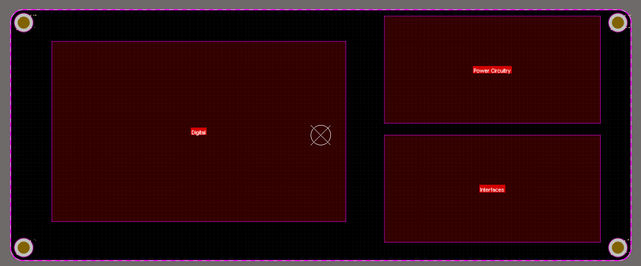
Going hand-in-hand with component placement is ensuring your board meets proper mechanical specifications in terms of its shape and mechanical features. Ensure that these items are set up before you begin any layout.
Routing Traces
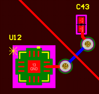
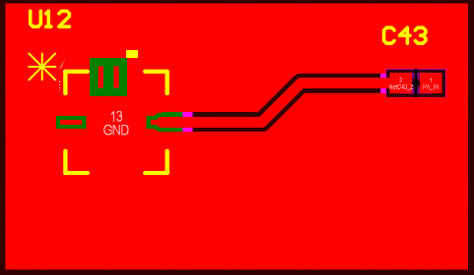
Once we have our components placed down, we begin the process of drawing tracks to connect them together. In general, we want to keep these tracks as short and direct as possible to minimize electrical loss and susceptiblity to electromagnetic interference
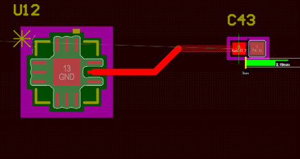
For any board with more than one layer, we additionally employ vias to connect traces through a board. Standard vias consist of a hole drilled through the board that is then plated with conductive metal. Traces on multiple different layers then can connect to this via in order to connect to each other.
Copper Pours and Planes
While routing traces between every component you will quickly find that for some common nets it becomes quite a tedious process. For example, the GND (ground) net is typically on a pad on every device on a PCB, and connecting all of them together using traces is both messy and cumbersome. Not to mention, these traces will create long paths to ground for each of these devices, which will form long conductive loops that can cause issues for our circuits - to be discussed next lecture.
To tackle this issue and make our routing lives easier, EDA softwares come with the copper pour feature. This tool allows us to define a region (e.g., the entire board outline) and have EDA software place a contiguous copper fill over all spaces without any copper originally (i.e., spaces where there are no traces, pads, or vias). This copper fill can be assigned to a particular net and made to automatically connect itself to other copper objects with the same net.
 Copper pour assigned the GND net.
Another way these copper pours are used on multi-layer boards is by having the pour occur on an empty layer and assigning it to a particular net. To have devices connect to the net, vias can be used to connect a pad to the poured layer (or plane). One will particular find this method (and copper pours in general) useful for global power nets and GND.
Appendix: Other Ways to Construct Circuits
Make no mistake! You don’t need a PCB to put circuits together! There’s a bunch of options for putting circuits together, depending on what exactly you’re trying to do. Here’s a handful of them:
Solderless breadboards
You might have seen these before, and they’re a great way to put together circuits for prototyping. They’re a block of plastic with a series of holes in them, and underneath the holes live a set of metal spring contacts that connect to the metal leads coming off of your part. By sticking your parts on the breadboard, the metal leads on your parts go inside the holes and make contact with the metal springs below. Doing this a bunch of times for all the parts lets you connect them together, and make a circuit!

Image Courtesy of Wikimedia Commons

Image Courtesy of SparkFun Electronics
These metal strips are arranged like shown - most of the strips are horizontal, but there’s some long vertical ones going down the side of the breadboard that are meant to be used for power, since a good bit of your circuit usually needs to be connected to power and ground.
While these are great for putting things together quickly and prototyping fast, circuits built on them don’t always last very long - after all, it’s just friction holding them in. And more importantly, not every circuit will fit onto a breadboard. Breadboards only work with through-hole components, which might cause problems for your circuit. A lot of components come in both through-hole and surface mount versions, but some are surface mount only, and don’t come in a through hole version. This affects chips (integrated circuits) the most, and so adapters like these are pretty common to make surface-mount devices breadboard-friendly:


Images Courtesy of SparkFun Electronics
Breadboards almost exclusively use a 0.1” spacing between holes, which is the spacing between leads on most through-hole ICs. Most through-hole ICs come in what’s called a DIP package (short for Dual, In-line Pins), which also uses the 0.1” spacing. DIP chips fit in 0.1” grids, which nearly all breadboards are.
Solderable Breadboards
These take the breadboard concept and turn it into something more permanent. They’re a specially laid out PCB that has a series of holes just like a breadboard does, but instead of connecting to the part with a spring, you solder to it. This means chemistry’s holding in your part instead of friction, and makes something that’s way more durable:


Images Courtesy of Adafruit and jmsaavedra
These are also known as a busboard, depending on who you talk to. These seem to be pretty popular in electronics education because it’s really easy to transfer a circuit on a solderless breadboard to a solderable breadboard. Solderable breadboards also have cousins called stripboard, which replaces the breadboard-style connections with strips that run down the entire board:

Image Courtesy of Wikipedia
Usually you don’t need the entire strip to make the connection, so you cut the copper on the board to the length you want. This stuff is also sometimes called Veroboard since Vero was the first company to make it.
Perfboard
These take a more free-form approach than the solderable breadboards do. These drop the bread-board like connections, and instead are just a grid of solderable holes. These are also called protoboards in some circles. In my experience, these are the most common in the real world.


Images Courtesy of Circuit Specialists, Jiří Praus, and osgeld
It’s also pretty common to route connections across the board by just adding solder across holes you’d like to connect, as shown above. Jumper wires that ‘jump’ across the board do the same thing too, just like we saw in breadboards and busboards. These also come in both 0.1” or 2mm grids - 0.1” is the most common, but some metric parts are on a 2mm grid.
Point-to-Point Construction
The ‘boards we’ve covered thus far are the most common ways to put circuits together, but there’s a few other methods that are worth mentioning, either for historical significance, artistic freedom, or just plain coolness.
Point-to-point construction falls into the former. It’s how circuits were assembled before the concept of a board emerged, and it’s quite simply just components soldered to each other in the shortest path possible. Larger mechanical parts were mounted to the case, but smaller things were usually just left floating. Here’s the insides of a 1948 Motorola VT-71 7” television to show what I mean:

Image Courtesy of Wikimedia Commons
As you can imagine, repairing or debugging this would be…not fun. But it worked! And circuits of moderate complexity were mass-produced by skilled workers using this technique.
Wire Wrapping
We eventually moved on to wire wrapping, which got popular in the 60s and 70s. Everything was mounted to a board, but the connections between modules were made by tightly wrapping wire around the legs of components. Doing this with the proper tool made a super tight, robust connection that looked about like this:

Image Courtesy of Jameco Electronics
This was used on big boards that had components on one side, and then wiring on the other. Here’s an example that shows this:

Image Courtesy of Nuts and Volts
This was extended to really, really, really large systems, like mainframe computers. Here’s what the backplane of a PDP-11 (the first machine to ever run UNIX) looks like. This was a computer the size of a few filing cabinets, and this is just one of its modules.

Image Courtesy of Trammell Hudson on Flickr. Click to zoom in on it, it’s a work of art.
Wire wrapped circuits were super reliable and serviceable - probing around inside a circuit was super easy since all the wires were exposed, and if you needed to adjust something, you could just unwrap the wire and move it. Despite this it had a limit on how densely it could be routed and manufacturing it was somewhat difficult to automate, so it fell out of popularity around the time the integrated circuit came on the block in the late 1970s. ICs work by routing a bunch of flat layers of silicon together to make transistors and connections between them - which is a design paradigm that’s exactly the same as our modern PCBs. Needless to say the mentality of ‘many flat layers connected together’ stuck, so now you’d be hard pressed to find anything other than a PCB in your electronics these days.
Free-form assembly
This technique doesn’t use any kind of structure at all, and really just lets your circuits flap in the breeze. Most of the time when Adi and I do this it’s because we’re lazy,[^1] but it’s a genuine art form when well-executed. I can’t think of a better example of this than The Clock, which is absolutely beautiful:

And Mohit Bhoite’s VU meter is adorable:

As is koogar’s headphone amplifier, which they set in epoxy resin:

Manhattan Style
Manhattan Style assembly works by cutting raw double-clad FR4 into a bunch of little squares, soldering those to a larger board, and then using those little squares as connection points in the circuit. This is best explained with a picture (actually from the same project as we saw the FR4 enclosure for earlier):

Image Courtesy of Dave Richards AA7EE
Since these small pads rise up from a bigger pad like skyscrapers, it’s called Manhattan Style. It’s really popular for prototyping RF stuff since it lets you space your parts however you’d like, and you get a big ground plane underneath everything. It’s not very compatible with ICs though, unless you flip the chip upside down in what’s called a dead bug arrangement:

Image Courtesy of IEEE Spectrum
In this case they’ve removed some sections of the top copper to make the isolated ‘islands’ that would otherwise be made with the small bits of stacked FR4 - but the principle is the same.