Lecture recording
00 — An Introduction, and Project Selections
We’re going to run things a little differently this year. Rather than everyone working on the same project, we’re going to let you pick your top 3 projects that you’d like to work on! We’d like you to let us know your selections via email or Slack (in your own channel, and mention @staff ) before lecture 01. We hope to have project assignments done about an hour after lecture 01. For full transparency, we’re assigning projects so our staff are spread evenly and not one staff member has to work extra due to the topics that are most popular. The projects that we have to select from are:
- Bluetooth RC Car
- Logic Analyzer
- MBTA Train Tracker
- Adjustable Power Supply
- Multimeter
- RGB LED Light
- FM audio radio receiver
- Wi-Fi Active Antenna
You can find a a more in depth description of each project here.
We’re also going to let you fab your own boards! This does make the first 2 weeks much tighter than last year, but we’re hoping that working on your own board helps you with developing your debugging skills.
Of course, we don’t expect everything to be 100% smooth. It’s the first time we tried anything like this. We ask that you stick with us, and be transparent about what’s not working. We’ll do our best to make sure the experience is as best as we can make it.
For the purpose of providing an example to follow, we’re going to be designing a smart RGB light.
01 - Defining Product Requirements
So we’re trying to build a product here. If you asked someone to describe what they want in a “smart light”, they will give you very different answers. A theatre lighting designer might want a 1000W PAR light that can move and create 16 million colors. A shop owner might want a tube light that can cover their entire shop in light. A 90 year old grandparent might say “out with all this smart stuff, just get me something that lasts for over a month!”. How do we design something when there’s that many different opinions on what we should design?
Enter, the product requirements. They are specifications set to better define what the product should be. In a lot of companies, this may be an entire document, often referred to as a PRD. They’re written in a way that ensures that everyone who works on the project are on the same page about what the product should accomplish. If you’re interested, Designing Electronics that Work has a much more rigirous definition and process for PRDs.
For us, let’s start by asking some questions about this smart light that will hopefully move us in the direction of a more defined product:
- What power source is being used?
- How do we control color and brightness?
- How bright should the light be?
Question 1 - What power source is being used?
Let’s create a chart to compare the pros and cons of different power sources
| Power Source | Pros | Cons |
|---|---|---|
| Battery | Can be used with wires | Needs charging, more complex |
| Solar | Free Energy! | Not much free energy, may need battery and circuit |
| USB-C | Abundant chargers | Must always be plugged in |
| Wall Power | Assessible and abundant power | Too dangerous to work with in our class |
Not much free energy is hard to quantify. How does one relate to that? We’re going to do some napkin math, and hopefully that will create a more concrete specification.
- Solar irradiance at the equator: 8kWh/m²/day
- For Boston? 5kWh/m²/day.
- Suppose we have a 0.1m x 0.1m panel. 50Wh/day
- Solar light -> electrical efficiency is 20%. 10Wh/day
- Not aiming right at the sun? 50% loss, 5Wh/day
- For context, a USB-C charger can supply 15W+.
- Solar takes a day to deliver as much energy as a charger does in 20 minutes. Solar doesn’t sound too appealing…
With a few hand calculations, we’ve determined a concrete answer for how much power is not much power.
So far, it looks like Wall Power and Solar are not viable options.
Let’s consider battery power. Do we want to replace AA batteries every few days? NO. So, let’s consider a rechargable battery option. It will probably have a USB-C charging port anyways, so we could layout a board with USB-C and a battery power option, but only consider the USB-C power section for now.
Question 2 - How do we control color and brightness?
Let’s walk through what a user would do in order to use the product.
- User opens phone and navigates to an app or website
- User selects a color and brightness
- The phone sends the data wirelessly to the light
- The light receives the data and converts the information into a control signal
One might notice: there is no mention of physical interaction with the light. What this suggests is that all the controls should be done wirelessly. In this user interaction study, we can conclude that our product needs Wi-Fi capability in order to be controlled by the user.
Question 3 - How bright should the light be?
To determine the ideal brightness for our smart light, we should benchmark existing smart lights. A lot of lights average around 8W of total power draw, and they advertise a brightness of 800 lumens. For us, let’s define a more broad range for our PRD: 100-1000 lumens of brightness. We also want to be able to change the color of the light, so let’s add a product requirement of producing a variety of colors.
Summarizing our product requirements
- Powered by USB-C
- Wi-Fi capability
- 100-1000 lumens of light
- Produce a variety of different colored light
02 - Defining Engineering Requirements
Now that we have our product requirements, we need to convert them into tangible specifications we can engineer for. Of course, some are less straight forward than others. For instance:
- Powered by USB-C
- Utilitze the 5V/3A standard of USB-C
- Wi-Fi capability
- How do we implement this?
- 10-100 lumens of light
- How does this translate to LEDs?
- Produce a variety of different colored light
- Red, Green, Blue, White strings of LEDs
It seems like we still have some questions about the engineering requirements. Perhaps answering them will help us better define the requirements.
Question 1 - How to implement Wi-Fi in a circuit?
The best way to answer this would be to look at what is already being done. There’s often no need to reinvent the wheel– a lot of problems are actually solved problems if you know how to look for them. So, searching for “Wi-Fi controlled lights DIY” gives us this Instructables guide on a DIY Wi-Fi RGB LED Lamp. This person uses an ESP8266 to handle the Wi-Fi communications. Let’s see if their solution may work for us!
We can look at the ESP8266 Datasheet to see what its features are. In the summary, the datasheet says this microcontroller contains:
- Wi-Fi functionality
- GPIOs (General Purpose In/Out. Basically, pins the microcontroller can change the state of)
That’s great! The microcontroller can receive Wi-Fi signals from the phone, and then change GPIOs accordingly. It looks like we have one solution!
Note: we’re actually using the ESP32 instead of the ESP8266. They both have similiar functionality and they’re from the same manufacturer, but we happen to have the ESP32 from last year.
Question 2 - How many LEDs?
We have a review on LEDs if you’d like a refresher before reading this section.
To start, we want all of you to learn to solder! It’s why we have this example project. Because of this, we want to have a lot of 1206 packages to practice on. Don’t worry too much about package sizes, we’ll cover those later this week. For now, let’s assume we’re using this 1206 LED.
It lists an 1800 mcd luminious intensity and a $115^{\circ}$ viewing angle. Does this mean anything? Perhaps. Googling for a mcd to lm converter shows this calculator, which suggests that the LED outputs 5 lm of light.
According to the datasheet, $V_{f} = 3.3V, I_f = 0.02A$. Let us suppose we put 10 LEDs in series. With 10 LEDs, it would output 50 lumens of light. We would need $10 \cdot 3.3V = 33V$ to drive the LEDs. A string would draw 0.02A at full brightness. This means the power draw would be $33V \cdot 0.02A = 0.67W$. Now, let’s duplicate that setup so there’s 4 strings: one for each color (Red, Green, Blue, White). This would total: 200 lumens of light, and a 2.64W power draw. It looks like this would meet our engineering specifications for brightness!
A schematic of the LED strings
A summary of our Engineering Requirements
Let’s summarize our results from Q1 and Q2 to see how our product requirements turn into engineering requirements:
- Powered by USB-C
- Utilitze the 5V/3A standard of USB-C
- Wi-Fi capability
- Utilize an ESP32 Microcontroller
- 10-100 lumens of light
- Utilize 4 strings of 10 LEDs each, driven at 20mA per string
- Produce a variety of different colored light
- Red, Green, Blue, White strings of LEDs
03 - Making a block diagram
03.00 But why make a block diagram?
Now that we have our engineering requirements laid out, let’s start putting them together to create one product! We’re going to start out with a block diagram. The blocks us visualize how different elements of our circuits will work together, without needing to modify circuits down to the resistor level. For now, we will abstract each block as doing a specific function.
The Speedee Service System video below is a great example of why we use block diagrams. Imagine if you’re in their shoes, and you had to create an efficient fast food restaurant layout. You could re-arrange all the appliances until you found the optimal setup, but that is expensive and time-consuming. Instead, they chalked appliances into blocks and had their employees pretend to use the layout. As they suggested, they got an efficient system within 6 hours, and without needing to move heavy appliances!
In the same way, circuit block diagrams help us re-arrange circuits without needing to modify every single part of a circuit. Maybe the block diagram doesn’t work because we realized throughout the process that the microcontroller needs more outputs than it has. Perhaps we notice that the delay through the different blocks would not meet our specifications. That’s okay! We would have to change a hypotethical rectangle we drew, instead of deleting entire circuits, or worse, ripping out entire physical circuits we built!
03.01 Creating blocks for the engineering requirements
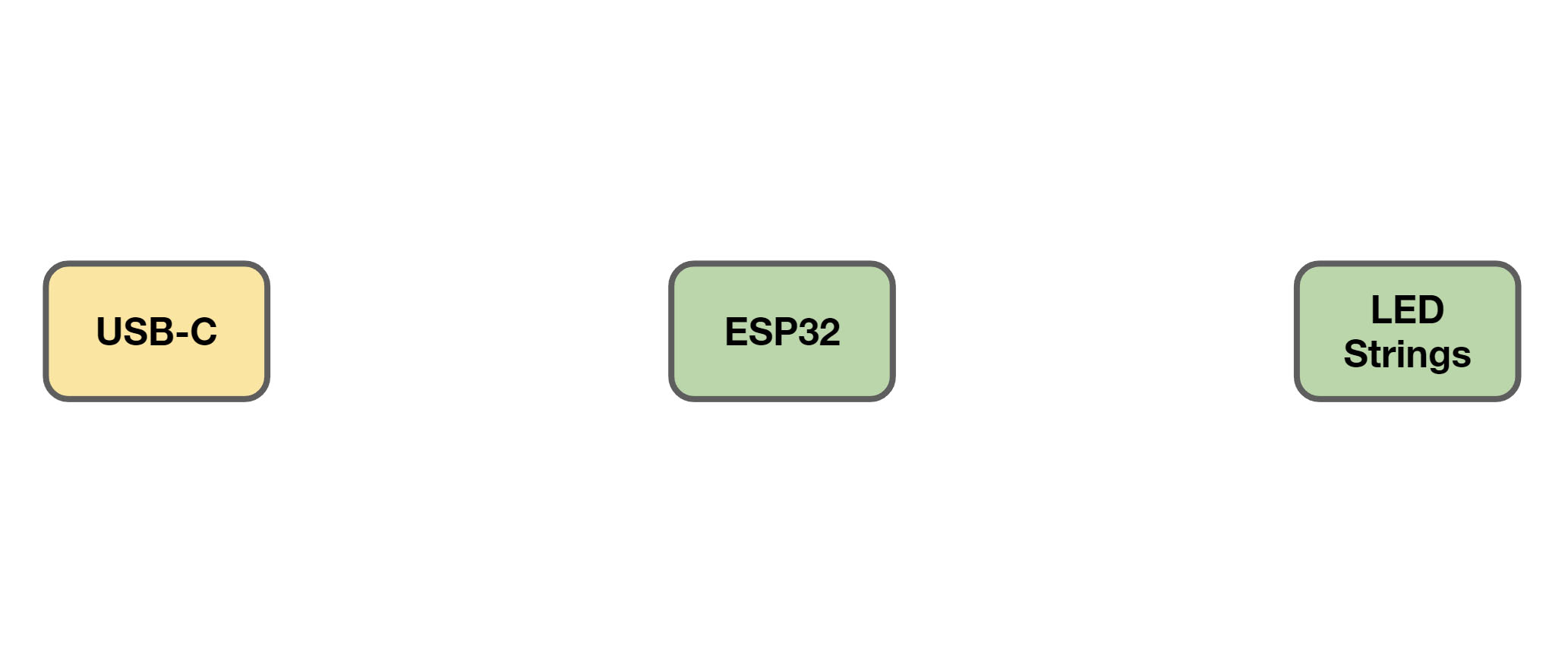
To start, let’s take the engineering requirements and convert them into blocks. Blocks should be comprised of a single function, such as LED Strings, USB-C, or ESP32. In this case, it makes sense to create a microcontroller block since we can’t really split the microcontroller into multiple blocks.
03.02 Adding transitional blocks
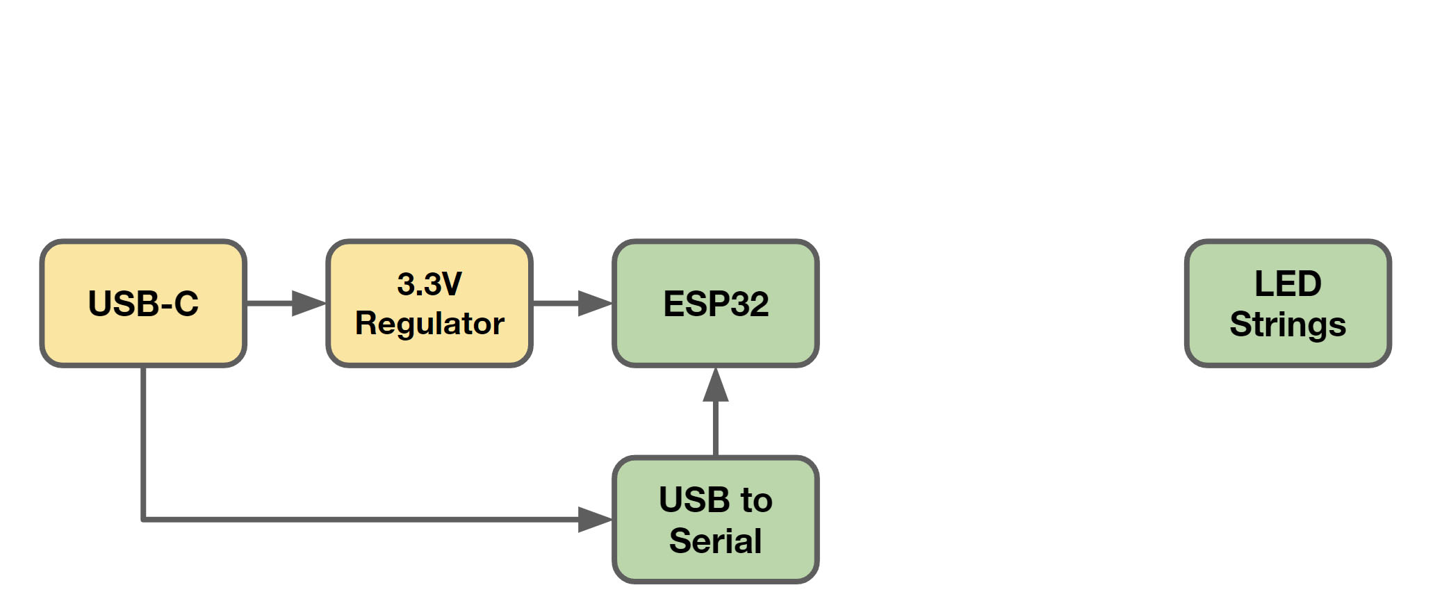
Let’s walk through the block diagram and see what needs to be added in order for the circuit to be functional.
You plug in the USB-C port. You expect the microcontroller to be powered and able to be programmed by your computer. This block diagram isn’t connected yet, so those actions can’t be performed yet. Let’s add some blocks in between so the microcontroller can be powered and programmed by the USB-C port.
-
Most microcontrollers nowadays need 3.3V, not 5V. The ESP32 is no different, and will require some regulator to produce the 3.3V rail.
-
Some microcontrollers will need a USB to serial bridge in order to be programmed. We call it a bridge since it connects the USB data of the USB port with the Serial data the ESP32 needs to be programmed.
Great, so let’s add a block for a 3.3V regulator and a USB to Serial converter. Notice the arrows, which signify the inputs and outputs of each block. The regulator gets power from the USB-C block, and outputs power to the ESP32 block. The USB to Serial block receives USB data from the USB port, and outputs Serial data to the ESP32. This is bi-directional, hence why the arrows go both ways.
Supposed to go both ways. Change your picture, bro
Now, we mentioned earlier that the LED strings need 33V in order to reach its full brightness. The USB-C port only provides 5V, so we’re going to need some converter that increases the 5V USB voltage to 36V to drive the LEDs. The extra 3V gives us some headroom to do some fancy controls and switching. Let’s add a block for a 5V to 36V Boost Converter– named because it boosts the output voltage to be higher than the input voltage.
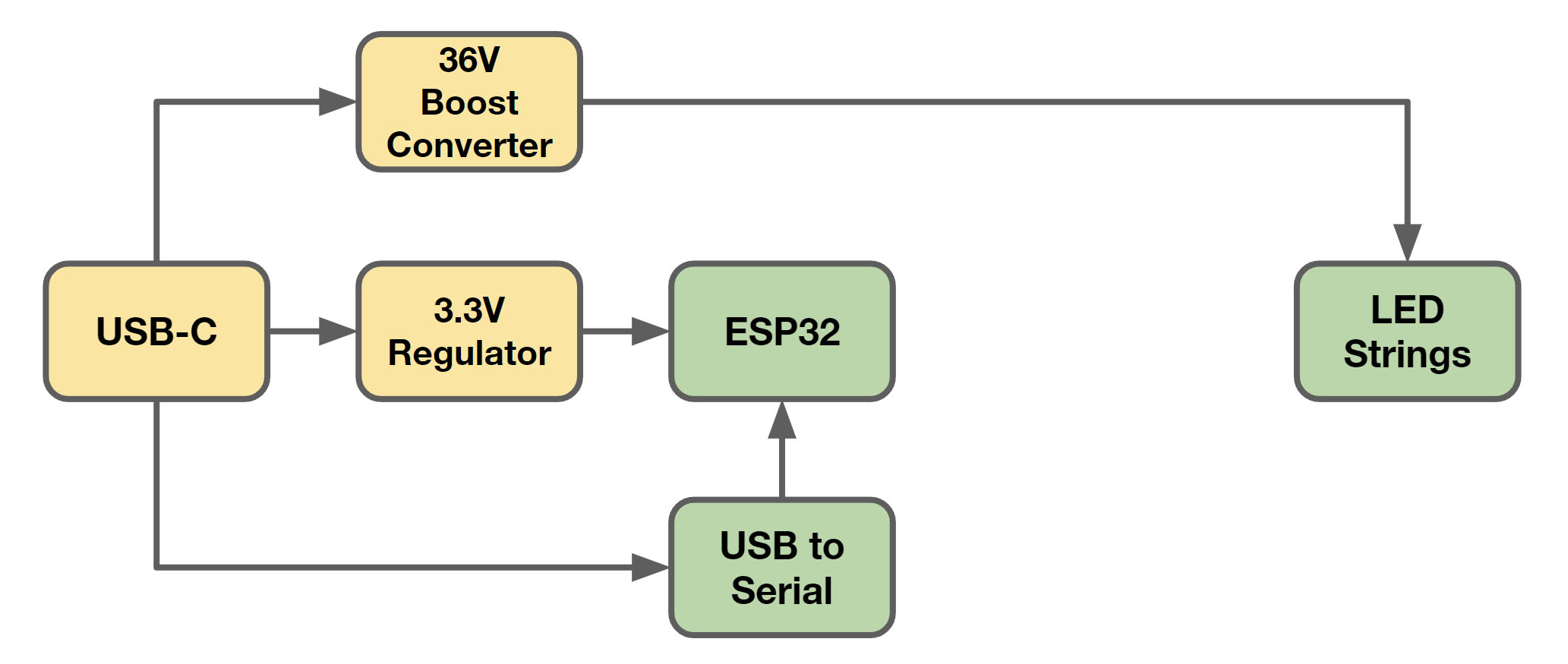
Unforunately, the ESP32 cannot directly drive the LEDs. Instead, we’re going to need some sort of magic that can drive the LEDs at constant current. Recall that LEDs have a very sharp current draw increase for a very small voltage change, which is why they’re driven at constant current and not constant voltage. Let’s add a block for an LED driver.
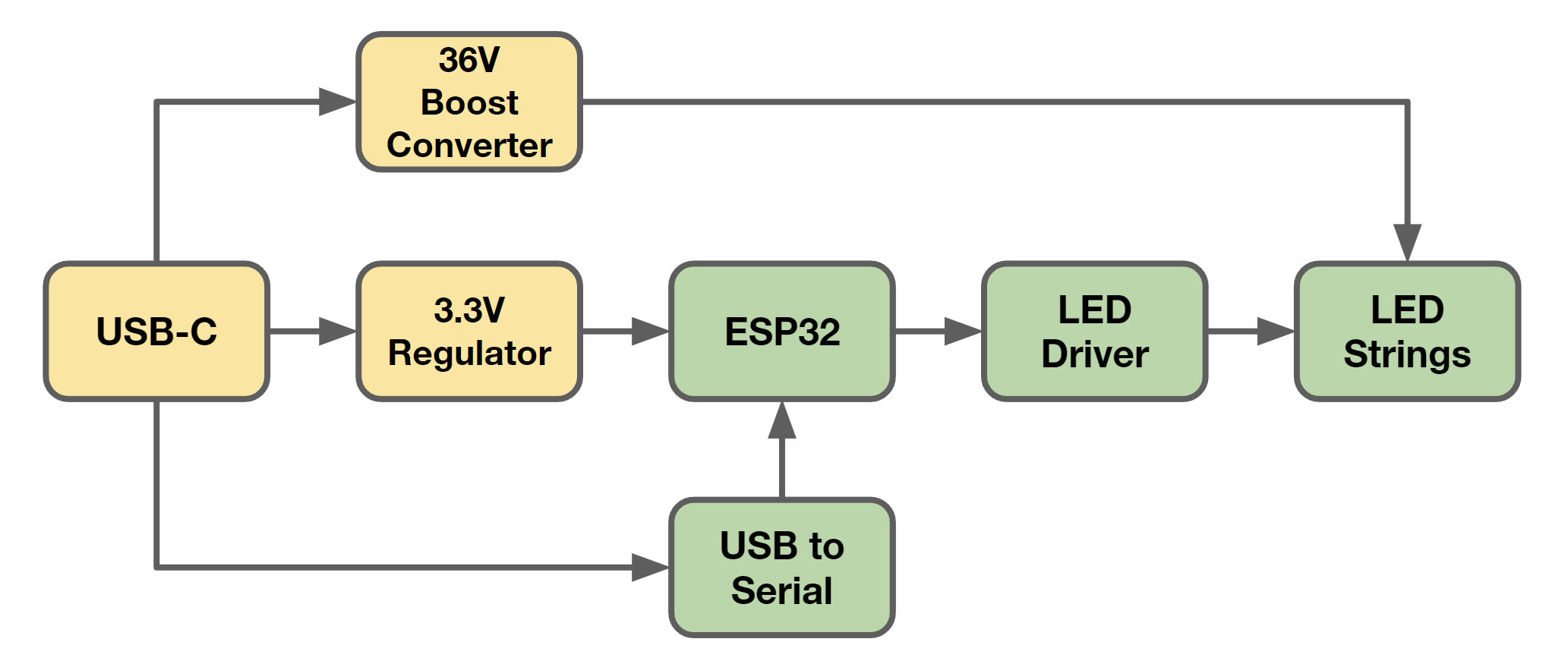
Cool, we have a full block diagram! But these are still blocks, where are the electronics that we’ve been promised?
03.03 Searching for example circuits
At first, this may seem complicated. You may be asking,
- How does one boost 5V to 36V?
- What exactly is a USB to Serial converter?
- What LED driver should we use?
The good news is, you’re likely not the first one to ask these questions! Lots of other people have all come up with solutions, and we can look at them for inspiration.
The Boost converter
For boosting 5V to 36V, this is a very common problem almost every PCB you make will need to work with. Maybe it isn’t these specific voltages, but lots of boards need voltage converters. Given how frequently designers need to solve this problem, lots of manufacturers created tools to make it easier for you (the circuit designer) to select what product to use! We’ll be using TI’s Webench Power Designer Tool to look at specific designs. This isn’t sponsored, we just happen to use it often since it offers lots of helpful features.
This is where the engineering specifications we defined earlier will come in handy. We said we need to drive 33V LED strings with a total current draw of 0.08A. Let’s round that up to 36V/0.1A for an output of our converter. Our input is a 5V USB source. When we look at designs that meet these specs, there comes out to be lots! Often times as engineers, we will need to sort our options to find a reasonable solution.
Let’s make the following assumptions:
-
We are lazy and we want as few components to solder as possible. Let’s sort for under 15 components. 15 is an arbitary number that’s chosen based on the distribution of component count shown on TI’s website.
-
We want a cheap solution, so let’s cap the cost at $3 for the entire circuit.
-
We’re going to rule out automotive-grade parts (marked with an -Q1 or similiar marking). They typically have the similiar performance metrics as consumer-grade parts, but go through more rigorous tests at a higher cost. We don’t need that high reliability, so the consumer-grade part will suffice.
Great, we’ve gotten down to 2 designs from 42! The two contenders are: the TPS61170, and the TPS61175. Here’s a comparison:
| Features | TPS61170 | TPS61175 |
|---|---|---|
| Soft Start | No | Yes |
| Programmable ${f_{sw}}$ | No | Yes |
| Iout Max | 1.2A | 3A |
| Component count | 10 | 12 |
| Total Cost | $1.61 | $2.54 |
Let’s qualify the features ans see which ones we need.
-
Soft start would be nice to have, but it’s likely not needed. Soft start works by slowly increasing $V_{out}$ so there’s no current spike. This is great for capacitve and inductive loads, but we don’t have that with the LEDs.
-
Programmable switching frequency is somewhat useful if you have sensitive electronics nearly. For instance, your 400kHz I2C communication line wouldn’t enjoy a 400kHz switching frequency from your converter. You might get interference between the 2 systems. The converter operates at 1.2MHz, so we can probably assume that nothing else will be at that frequency. Hence, we don’t need the programmable switching frequency.
-
Maximum current output of over 1.2A. This number is slightly confusing. What they actually mean is the switch inside the IC should not exceed 1.2A. Marketing… Anyways, TI’s simulation shows the IC would pull 0.9A on the switch at full load of 0.1A output, so we should be good with the TPS61170.
Those three features are the main reason why one might choose the TPS61175 over the TPS61170. Since we don’t need those features, we can save 2 components and the $1 and go with the cheaper TPS61170.
The tool also gives us an example circuit with pre-selected components, how convinient! Let’s save a picture for now, it might come in handy.
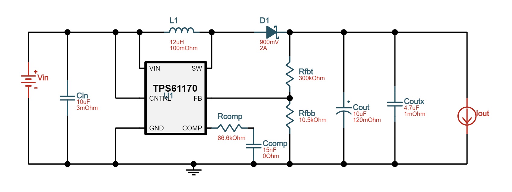
TPS61170 Schematic from TI (You might need a TI account to see it)
ESP32 Example Circuit
For the ESP32 circuit, we can also search to see if others have made a USB powered circuit with a programming circuit. And will you look at that! Expressif, the manufacturer of the ESP32, makes their own development boards that have this function! It’s almost like they want to help us use it! Development boards for specific ICs are fairly common for manufacturers to make, so they’re usually a good start for how to implement a certain chip. They may even have schematics that show how they implemented their own chips! How convinient! Let’s look at their schematic, and copy down their USB to Serial solution, as well as their 3.3V regulator design. And there we go, we have a example schematic for 2 more blocks.
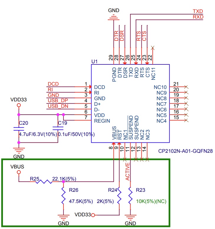
USB to Serial Converter from the ESP32 DevKitC V4 Schematic
3.3V Regulator from the ESP32 DevKitC V4 Schematic
USB-C Implementation
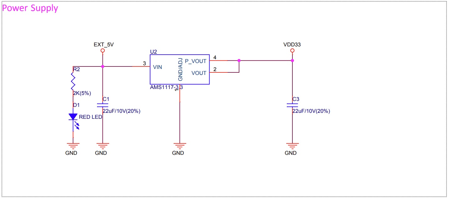
Likewise, Adafruit has ESP32 development boards that have USB-C! We can look at schematics from Adafruit, and they can help give us an idea of how to get 5V/3A using USB-C.
USB-C Recepticle circuit from the Adafruit ESP32 Feather V2
Constant Current LED Driver
We have a crash course on MOSFETs if you’d like a refresher before reading this section.
We know that we need some constant-current LED driver for our LEDs, as the current is what determines the brightness. This is because the voltage drop across the LED stays roughly the same regardless of the current draw. We can do a Google search for constant current drivers, though we have to be careful since Google tends to have some level of misinformation out there. We often like to qualify a schematic that’s by random people before using it. Does it pass a first check? Let’s verify this constant current driver we found on the $internet ^{TM}$.
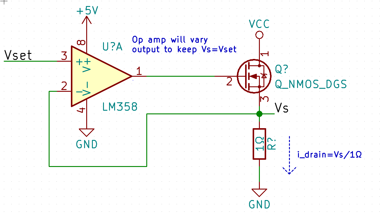
Constant Current SInk from Learn CNC
Starting from the left, there’s a Vset voltage. It goes into the non-inverting port of the op-amp. The op-amp will attempt to adjust the output until the inverting port of the op-amp is equal to the non-inverting port. Let’s say V+ > V-. The op-amp will output a higher output voltage, raising the gate voltage of the N-channel mosfet. This will allow more current to flow from VCC to Vs, and hence Vs to GND. The resistor is a “shunt resistor” that measures the current draw and converts it into a voltage. Since the current through the resistor increases, Vs increases, and creates negative feedback to the op-amp. This seems to work! It’s not perfect, as the parts aren’t selected. But it’s a good start, and we can save this schematic for later use.
Appendix
A review on LEDs
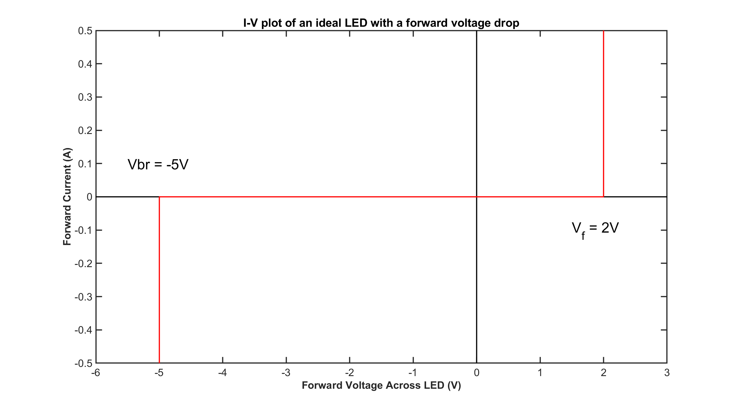
You might recall from 6.2000/2.678 that LEDs don’t have a defined current draw at a specific voltage. An ideal LED with a forward voltage drop would not allow any current flow until the voltage across the LED reaches its forward voltage ( $V_{f}$), and then lets infinite current through once past its forward voltage. As you can see on the graph, the current across the LED is 0A from 0-2V. Once the forward voltage goes beyond 2V, the current through the LED goes up to infinity.
But what about the bit where the current drops to negative infinity at -5V? That’s called the reverse breakdown voltage ($V_{br}$). For LEDs it’s typically -5V, and other diodes may have ratings from -10V to well over -1000V, depending on application. We won’t have to worry about it here, but just know that most diodes, with the exception of zener diodes, die after they hit reverse breakdown.
With real LEDs and diodes, they’re slightly different. Rather than an infinite sloped I-V curve, it’s an exponential curve. This often means that $V_{f}$ is a bit higher to define. The typical definition for $V_{f}$ is the voltage where the LED will be conducting a current of $I_{f}$, or the forward current. $I_{f}$ may be the current they test the LED with, or the maximum current of the LED. Check the datasheet as always for the manufacturer’s definition.
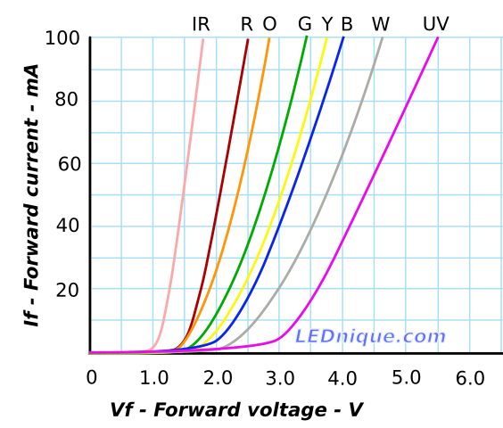
In theory, this means you could control the LED’s power output (and thereby brightness) using constant voltage. The slope of the I-V curve around the region of interest is about 200 $\frac{mA}{V}$, so you’d just have to be very careful about the exact voltage you apply to the LED, down to 0.01V or less if we want an accuracy of 2mA. A typical indicator light for debugging is fairly bright at 1mA, and most LEDs that aren’t for lighting are rated for 20mA or less. Except… $V_{f}$ decreases with temperature! It’s also highly variant across multiple batches. Welcome to the world of nonlinear systems. It’s like if you strapped a jet engine to your bike and tried using the throttle to go at walking speed. You could try, but more likely, it’s not going to be stable.
If we want to control is with any reliability, we’re going to need to decrease that I/V slope or use a feedback system to precisely set the voltage with mV or sub-mV accuracy. If you haven’t guessed already, most LEDs don’t have such control systems. Instead, they use a simple resistor in series with the LED. The intuitive way to think of it is:
- At low voltages (below $V_{f}$) the LED doesn’t let current through
- At higher voltages (way above $V_{f}$) the resistor is the limiting factor for current
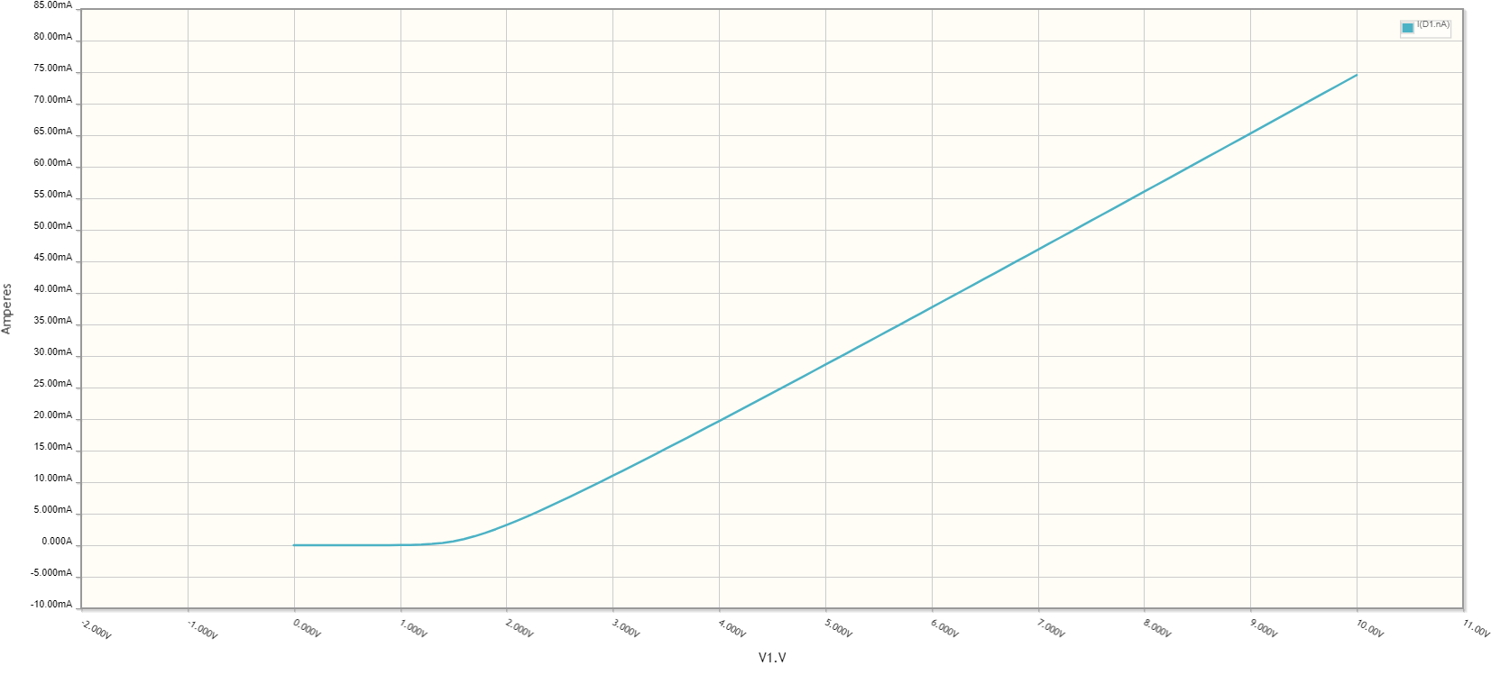
Let’s look at an actual I-V plot with a generic LED in series with a 1K $\Omega$ resistor. The slope of that line is roughly 10 $\frac{mA}{V}$, so it’s much easier to control the current across the LED!
A crash course on MOSFETs
MOSFETs are an amazing invention that makes today’s electronics possible. They’re semiconductor switches that power everything that’s electronic. Let’s explore how they work!
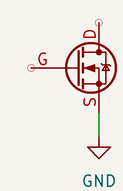
Picture this: there’s a faucet knob in front of you. When you turn the knob, water flows out. It’s a switch! The MOSFET is the same way. When we apply a different voltage to the gate (G) relative to the source (S), it’s like turning the knob. As a result, a controlled amount of current flows through from the drain (D) to the source (S). Pictured below is an N-channel mosfet. There are P-channel and N-channel mosfets, but we’re going to focus on N-channel mosfets for now. You might notice the source is connected to GND. It will make our math a little easier, so we can refer to the gate-source voltage as the gate voltage from now on.
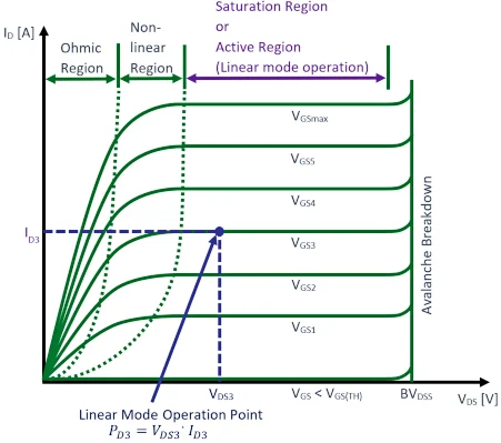
The Ohmic Regime
Let’s say that we opened the faucet all the way. The more water pressure there is feeding into the faucet, the more water will be flowing through. In the same way, we can turn on the mosfet by applying a large voltage (10V) to the gate. For small currents, $V_{DS}$ and $I_{D}$ are proportional. This sounds a lot like a resistor, where V and I are related by a constant, R! For this reason, this is the Ohmic region of the mosfet. \ The datasheet usually lists this resistance, known as $R_{DS_{ON}}$ since it’s resistance between the drain and source when the mosfet is on. Note that the slope is slightly different for different gate voltages, hence $R_{DS_{ON}}$ ratings are usually given with a gate voltage. A higher gate voltage results in a lower $R_{DS_{ON}}$. When we’re using the mosfet as a switch, we’re going to want to be in this regime. Why? Because the conductive losses in the mosfet are $ V_{DS} \cdot I_{D}$. The ohmic region is the closest to the origin, and hence where both $ V_{DS}$ and $I_{D}$ are lowest.
The Saturation Regime
Let’s picture another scenario. We’re going to connect a firehose to the inlet of the faucet. The faucet will now be opened a very small amount. No matter what the pressure is that’s behind the faucet, the small opening means there’s a certain amount of water that can flow across. We could control the amount of water that comes out by varying how open the faucet is. Same with the mosfet. If we apply a small voltage to the gate, then only a small current can flow through the drain -> source. When the gate voltage is increased, then more current can flow. On the graph, $V_{GSn}$ represents an increasing set of gate voltages. As the gate voltage increases, more current is able to flow. You might notice, the curve is flat at the saturation regime– demonstrating how the drain-source voltage does not affect the drain current. This region is great for analog controls for varying the current through the FET, and the gate is usually tied to an op-amp or other amplifier. It’s not great for efficiency though, since the high $V_{DS}$ can lead to a high power loss in the mosfet.
The Avalanche Breakdown Regime
Mosfets have a maximum $V_{DS}$ rating, named $BV_{DSS}$, or the Drain-Source breakdown voltage. Don’t dare go near it, or the mosfet dies. See how the current shoots up at the avalanche breakdown? You’ve just created a really expensive short. Mosfets often will fail to a short, so if you’re pushing the limits, keep that in mind.
Switching losses
With your faucet, you need energy to turn it on or off. Once it’s in an on or off state, it stays that way and you need very little energy to keep it in that state. Same with the mosfet. Because of the way mosfets are manufactured, there’s a very small capacitance between the gate and the drain, as well the drain and source. This capacitance needs to be charged or discharged every time a switching event happens. In datasheets, you can find the total gate charge, and it’s a good approximation for the number of electrons that need to be shuffled around during a switching event. Let’s call total gate charge $Q_G$. This means it takes time to switch a mosfet, as you can’t drive the gate with infinite current. Gate driver ICs exist for this reason– if you need to switch very fast, or you want a higher gate voltage than what you can get from a microcontroller, gate drivers are the way to go. They can shove 10V/1A easily into a mosfet’s gate rather than a measly 3.3V/0.01A from a microcontroller. We can estimate the mosfet switching time as $t_{SW} = \frac{Q_G}{I_G}$ (The time for $I_G$ to exchange a charge of $Q_G$). Assuming this is a turn-on switch, the mosfet goes from non-conductive, to saturation, to ohmic (if you designed it to be in ohmic in steady state). Remember that the saturation regime is very lossy? That’s going to cause some problems. Let’s calculate that loss.
We know that $V_{DS}$ has to go from $V_{DS_{MAX}}$ to ~0V, and $I_{D}$ has to go from 0A to ${I_{D_{MAX}}}$. We can roughly assume they linearly decrease/increase. The instantaneous power loss is a function of ${I_D} \cdot V_{DS}$. Let’s approximate the peak switching power loss as $P_{SW_{peak}} = V_{DS_{MAX}} \cdot {I_{D_{MAX}}}$. The shape of the switching loss curve is a triangle with width $t_{SW}$ and height $V_{DS_{MAX}} \cdot {I_{D_{MAX}}}$. Recall that $\int Power \cdot dt = Energy$, and the area under the curve is the integral. Hence, the energy loss for turning on the mosfet once is
$\frac{1}{2} \cdot P_{SW_{PEAK}} \cdot t_{SW}$
$= \frac{1}{2} \cdot V_{DS_{MAX}} \cdot {I_{D_{MAX}}} \cdot \frac{Q_G}{I_G}$
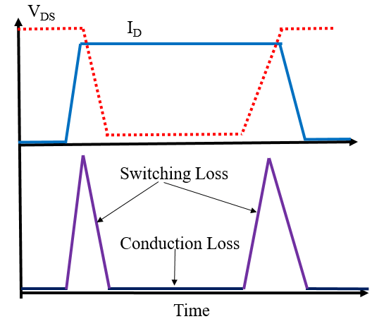
Mosfet losses during switching
Turn-off is a similiar calculation and one can assume the loss for turn-on is about equal to the loss for turn-off. This equation is not perfect– there’s some effects like the miller plateu that changes this number slightly, but we’re using it as a rough overestimate. But we’re not switching it once in most cases! If we’re switching it at frequency $f_{SW}$, then the switching loss would be:
$f_{SW} \cdot V_{DS_{MAX}} \cdot {I_{D_{MAX}}} \cdot \frac{Q_G}{I_G}$
Total losses
Don’t forget, we have conduction losses too since the mosfet as a drain-souce resistance!
$R_{DS_{ON}} \cdot I_{D_{peak}}^2 + f_{SW} \cdot V_{DS_{MAX}} \cdot {I_{D_{MAX}}} \cdot \frac{Q_G}{I_G}$
How do we create a more efficient switch?
- Choosing a different mosfet gives better figure of merits ($R_{DS_{ON}},Q_G$ )
- Switching at a lower frequency reduces switching losses
- Using a better gate driver for higher $I_G$ or a higher gate voltage for a lower $R_{DS_{ON}}$
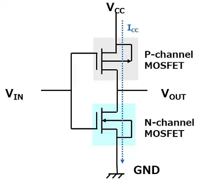
On P-Channel Mosfets
Oh right, there’s still the P-Channel mosfet. It’s almost the same as an N-Channel mosfet, except a negative gate-source voltage turns on the mosfet. Weird, right? It’s like a screw you turn left to tighten it. It seems like a weird child. It’s inferior in many ways. P-channel mosfets often have worse figures of merit compared to a smiliar N-channel counterpart, and they’re more expensive. They have their uses though. Imagine you want a high-side switch, where the source is connected to +V instead of ground. with an N-channel mosfet you’d need a voltage higher than +V to turn it on, whereas a voltage of 0V would likely turn on the P-channel mosfet. This makes a P-channel very useful if we don’t want a secondary power source for the gate circuits, and they’re often used in CMOS design. With the two C omplementary MOS fets, we can make an inverter. This deisgn is very typical for the output for many ICs, as any current drawn by VOUT goes through the mosfets rather than the VIN signal.