Suggested Reading
- Chapter 5 of Designing Electronics that Work covers Layout design. Don’t worry too much about 5.2 Performance, as most of us are not working with RF/microwave stuff currently.
Re-arranging the default placement
The layout tip of sectioning out components into similar rooms is a good starting point but it leaves out how each component itself should be placed and routed. To figure out how to arrange individual components, we can start by laying out critical devices (e.g., power regulators, microcontrollers, ICs). These components will often have a recommended layout provided by the manufacturer at the bottom of their datasheet. They are not perfect and may not fit for every application of the device, but they are made by people who know a lot about the component. Here’s a layout example from the TPS61170 which is being used for the demo board you will be soldering in lab 3. The re-coloring is for ease of visualization.
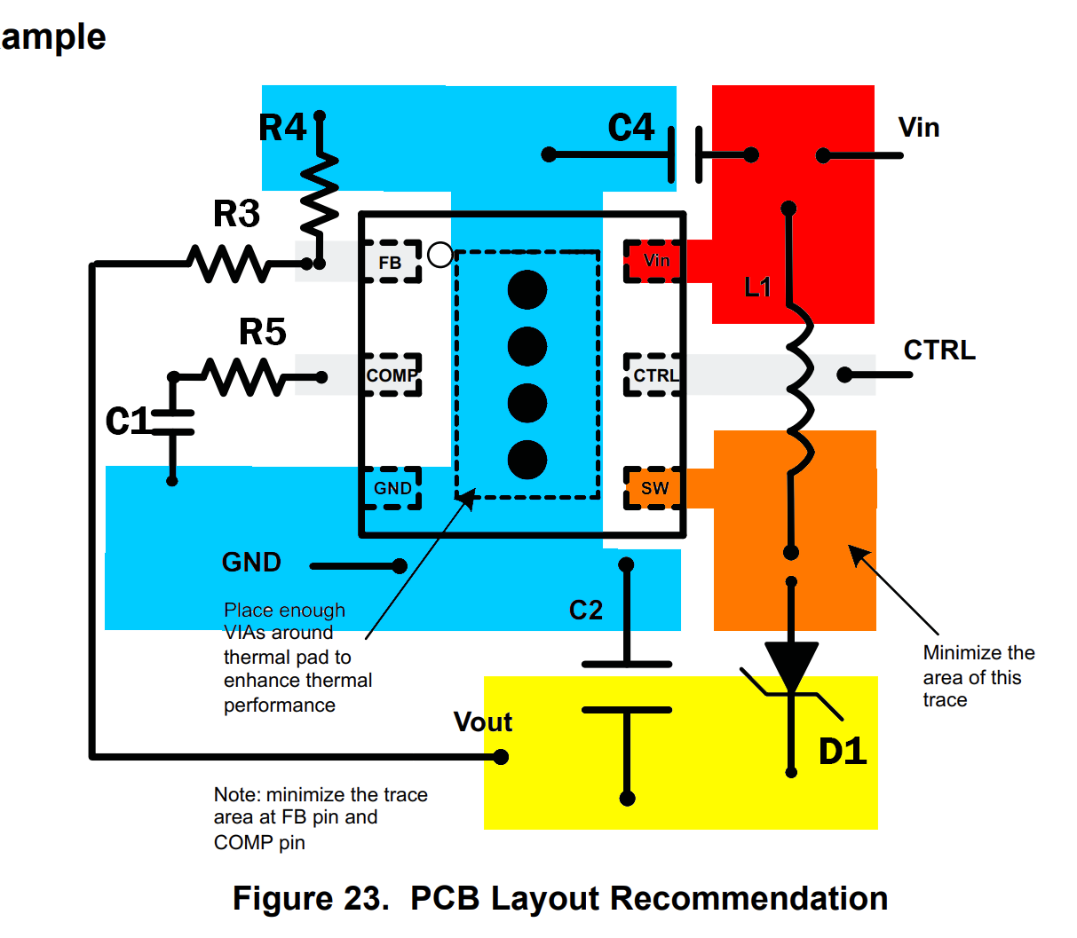
Image Credit: TI
Editing: Winnie Szeto
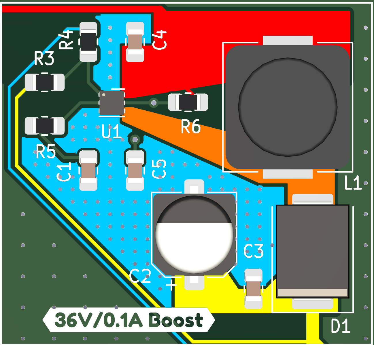
Typically, each of your blocks in your block diagram should be centered around one (or two) IC(s). Those are the ones that you will want to look at the recommended layout for in its datasheet. For the rest of the components you can arrange them such that they fit around main IC(s) to optimize routing and avoid crossovers as much as possible.
Do not get attached to a layout
It is very tempting to want to stick to layout that you have been working for a while (the sunken costs are tempting!). But often times, your first layout will contain errors and mistakes that you learn of later on. And for that reason, it may often be best to rip up your current progress and start over, rather than continuing off of what you already have. If you want a metric for when a layout becomes beyond saving, ask yourself: if I were to rip it up, would I eliminate any constraints that are put down by my current layout? You might for instance have a lot of wires crossing, and as a result, there’s not an easy way to go across. If that’s the case, you may want to consider re-routing things.
ESP32 Considerations
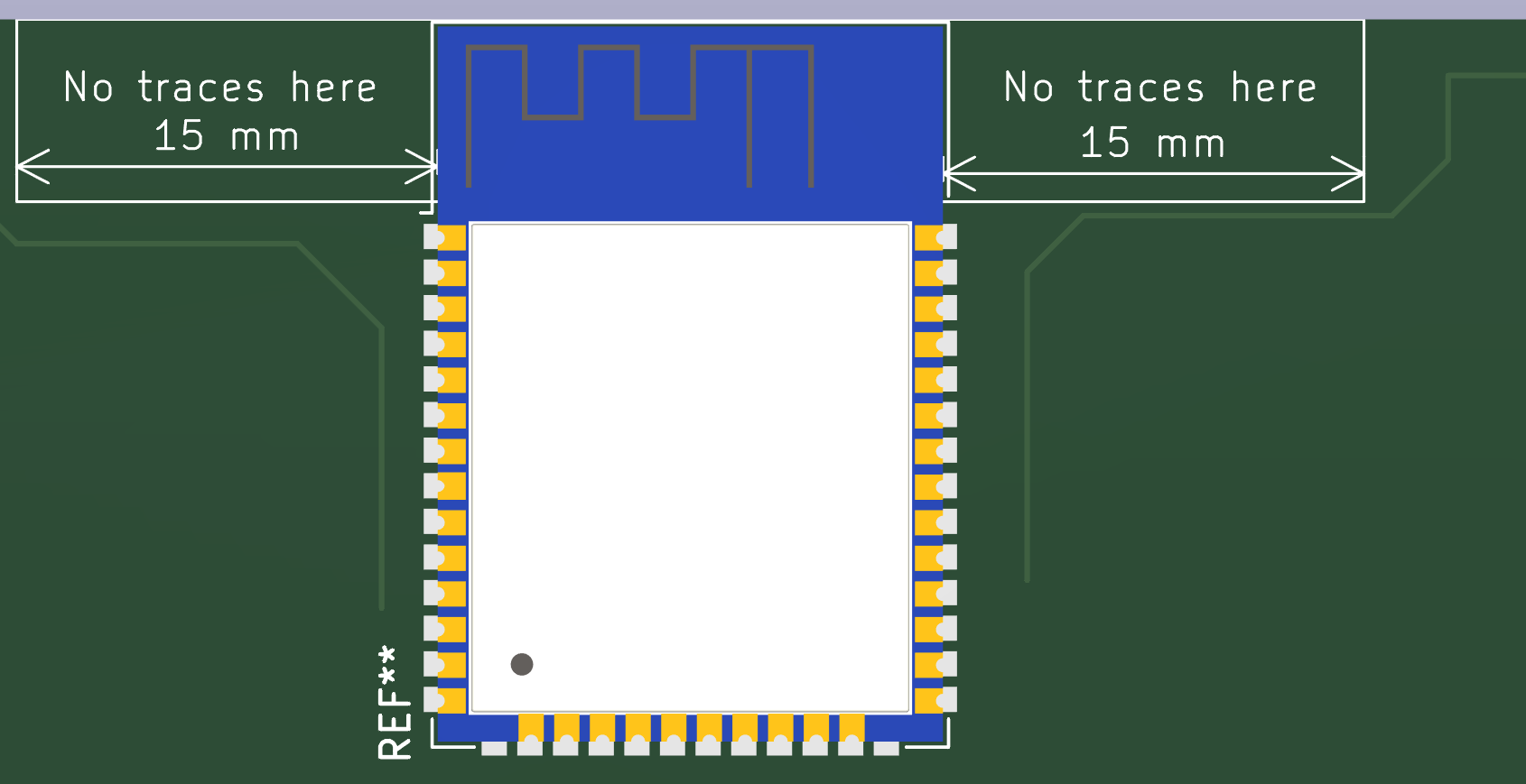
If you are planning to use the wireless capabilities of the ESP32-S3-WROOM, then we suggest you follow their guidelines for layout. Expressif has a guide on how to place the ESP32-S3-WROOM, which you can find here. The feed point for the module we are using is on the right side.
In reality, a lot of designs are not always able to follow the manufacturer’s guidelines **exactly**. Take a look at Adafruit’s designs as an example.
Expressif (the makers of the ESP32) recommend not having any traces within 15 mm of the left and right of the ESP32’s antenna. The Adafruit board below looks as though it has traces a much closer than 15 mm to the antenna, but they did at least create a region where there are no traces immediately next to the antenna.
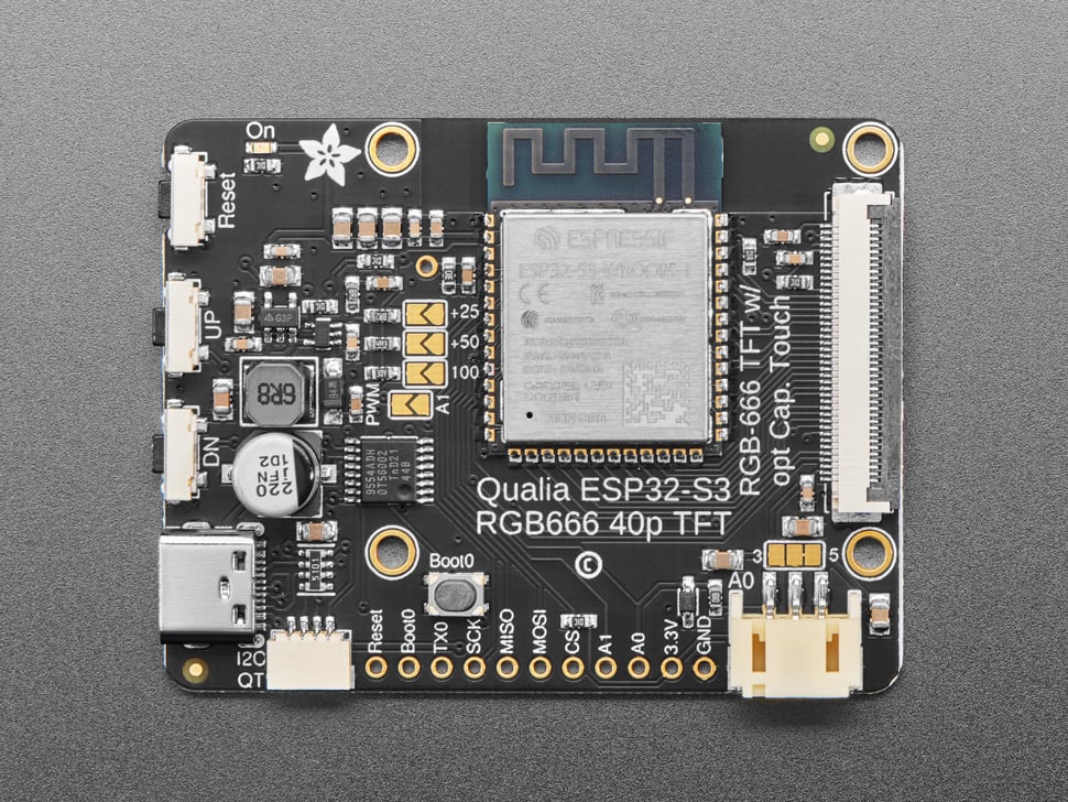
Image source: Adafruit
The next image is definitely going against the guidelines that Expressif specifies. The USB port and barrel jack are quite close to the antenna, and it is likely that this design will affect the emission pattern of the ESP32’s Wi-Fi antenna from what Expressif designed it to have.
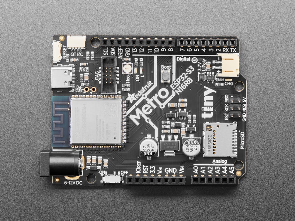
Image source: Adafruit
This raises the point of how the recommended layout for a device is only but a recommendation. The Expressif guidelines are designed to ensure the antenna emission pattern will retain the performance guarantees found in the ESP32 datasheet, but often such is not a requirement for our designs. It’s all based on what your PCB needs to meet its performance benchmarks. From our experience, we suggest you at a minimum:
- Move the outside edge of the antenna to the board edge
- Leave 15 mm of space between the antenna and any traces or bits of stuff
If you are not putting traces next to the antenna, you might as well cut out the whole board substrate!
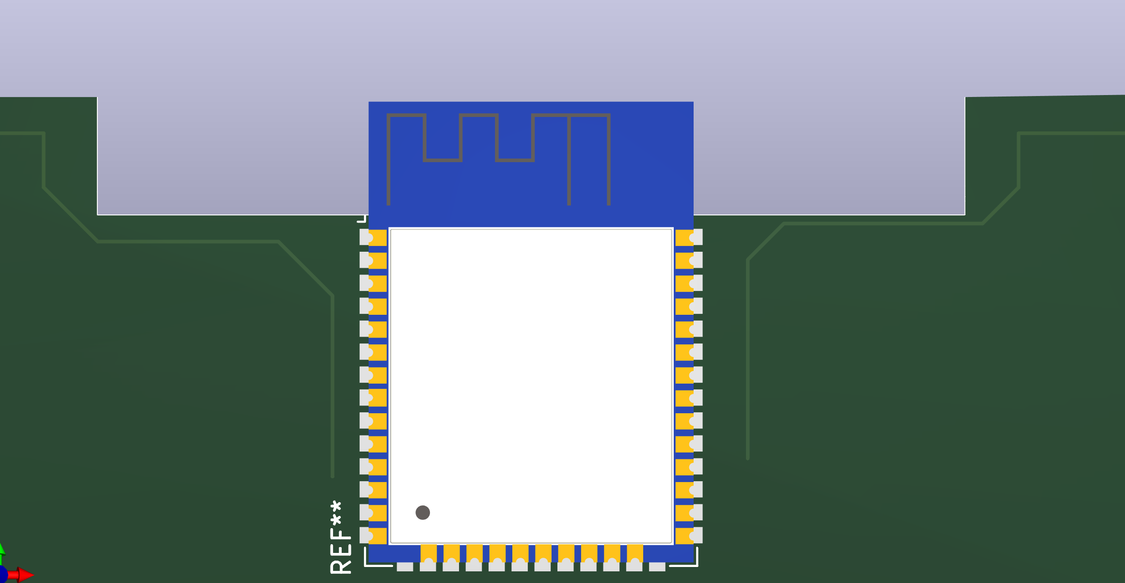
Even better, you could even do what we did in our demo board, which is let the antenna stick out.
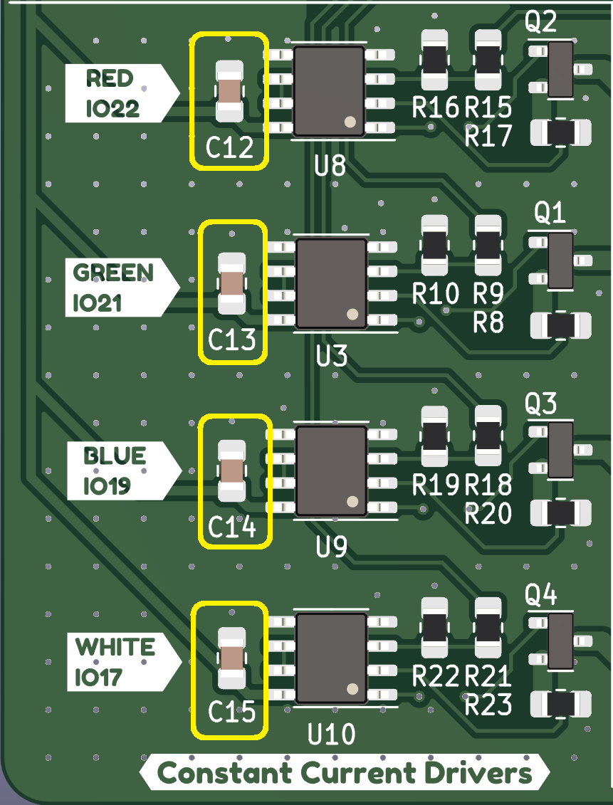
And as a reminder, most pins that were assigned to the ESP32-S3 were done so semi-arbitrarily. This is made possible by the ESP32-S3’s GPIO multiplexer, which allows mapping most I/O to any pin using software. What this means is that you can use program GPIO pins in ways that make routing easier! You can see in our example we switched around which ESP32 GPIO pin was R_SIG, G_SIG, B_SIG, and W_SIG so that routing becomes most convenient for us. We suggest you do the same to make it easier on yourself, but note that not every GPIO pin can support every I/O function provided by the ESP32. Here is a good resource on which pins can be used for what but the main points are:
- Do not use GPIO 0, GPIO 45, GPIO 46 for anything (GPIO 0 should be routed to a button to GND for boot control)
- GPIO 19 and GPIO 20 should be routed to USB Data - and USB Data + respectively
- If you need to read a voltage’s value (i.e., 1.5V, 2.5V and not just High/Low) use an ADC1 pin (Analog to digital converter). ADC2 cannot be used while Wi-Fi is being used
- We will not be using JTAG debugging, Octal PSRAM, or EFuse burning in this class so do not worry about those interfaces
No unrouted traces
In KiCad’s PCB editor, you can find an “unrouted” trace count in the bottom left. This should be at 0 when you’re done routing. If you can’t find the unrouted trace, use DRC to find it for you.
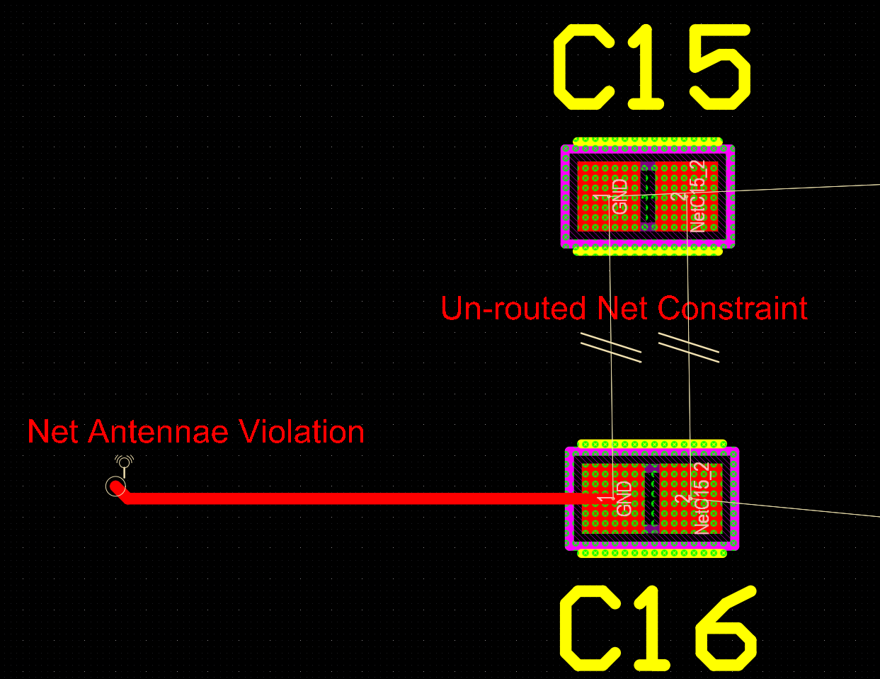
In Altium, unrouted nets will be shown via ratsnest line and after a DRC is run, each will be marked with a Un-routed Net Constraint (depicted with a capacitor below) or with a Net Antennae violation (depicted with the circular antenna below) for unfinished traces.
Decoupling capacitors
These should be placed next to every power pin on every IC as close as possible. Decoupling capacitors are 100nF - 1uF capacitors that filter out noise and undesired transients from the power supply.
Footprints
Check all footprints against their respective schematic symbols and datasheet. Ensure the pads on the footprint match the pins on the symbol.
Mechanical Considerations
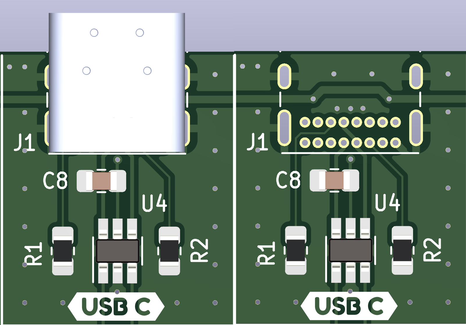
For those using a USB port, in order to actually be able to plug a USB cable into it, the port cannot be blocked by the board’s edge. Pay close attention to the line on the USB connector’s footprint that says “BOARD EDGE” as that is will need to line up with the board edge. The connections on the through-hole pads should be made on the board and not in midair. Yes, this does sounds obvious, but there are some of us who forget and place it backwards. The same goes for headers and other connectors - consider how someone where and how someone may plug something into a connector and ensure nothing blocks insertion and removal. This is another reason why your PCB EDA software’s 3D view is essential for board verification.
Mounting holes are also important. How will the board fit in an enclosure? How close are parts to the board edge? MLCCs (small capacitors) in general do not like to be < 5mm from a board edge because they could crack easier and short out from mechanical stress.
Do you have enough space to press the buttons on your board?
Are all the test points you put down easily accessible?
Do you have sharp edges on your board? If so, consider using a fillet or chamfer. A rounded edge is much less sharp than a square edge, and it will hurt a lot less if you end up getting stabbed by it.
Although nobody will be using accelerometers in this year’s class, make sure they are placed near a mounting hole! They often have specifications that require them to be attached near a hard mounting point because boards can flex and cause sensor noise issues.
Fabrication Constraints set correctly
Your board must be bigger than 25mm x 25mm and be no larger than a 100mm x 100mm square. This is a constraint set by how fast PCB fabs can make a board. Anything bigger or smaller and it takes longer. On the same note, we’re making all boards to be 2 layer, green solder mask. If you want a thickness that isn’t 1.6mm, talk to us and we’ll consider.
Trace width and spacing
On KiCad:
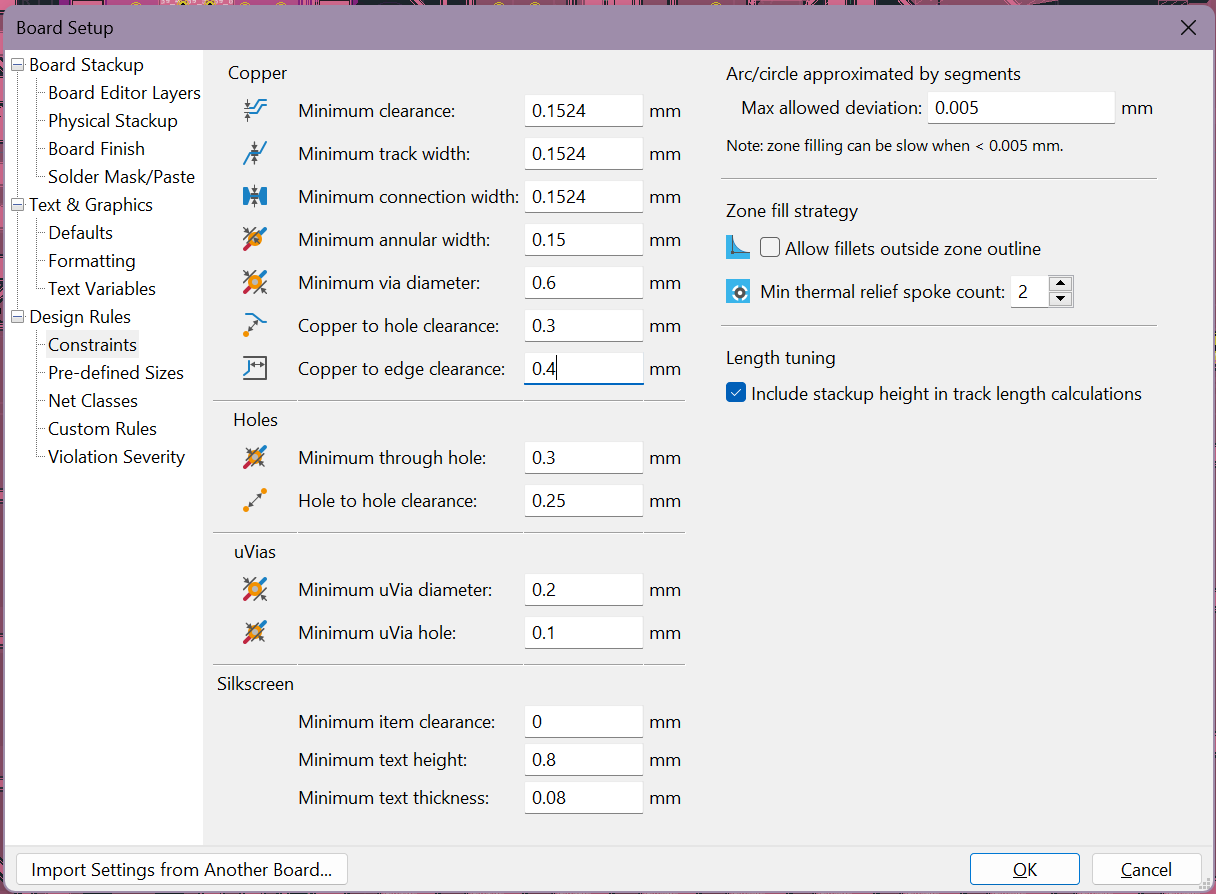
- Go to File -> Board Setup to open Board Setup
- “Physical Layers” has 2 copper layers (for this class we’re using 2-layer)
- Constraints set as such:
- Minimum clearance: 0.1524 mm
- Minimum track width: 0.1524 mm
- Minimum via diameter: 0.6 mm
- Copper to hole clearance: 0.3 mm
- Copper to Edge clearance: 0.4 mm
- Minimum through-hole: 0.3 mm
- Hole to hole clearance: 0.25 mm
On Altium:
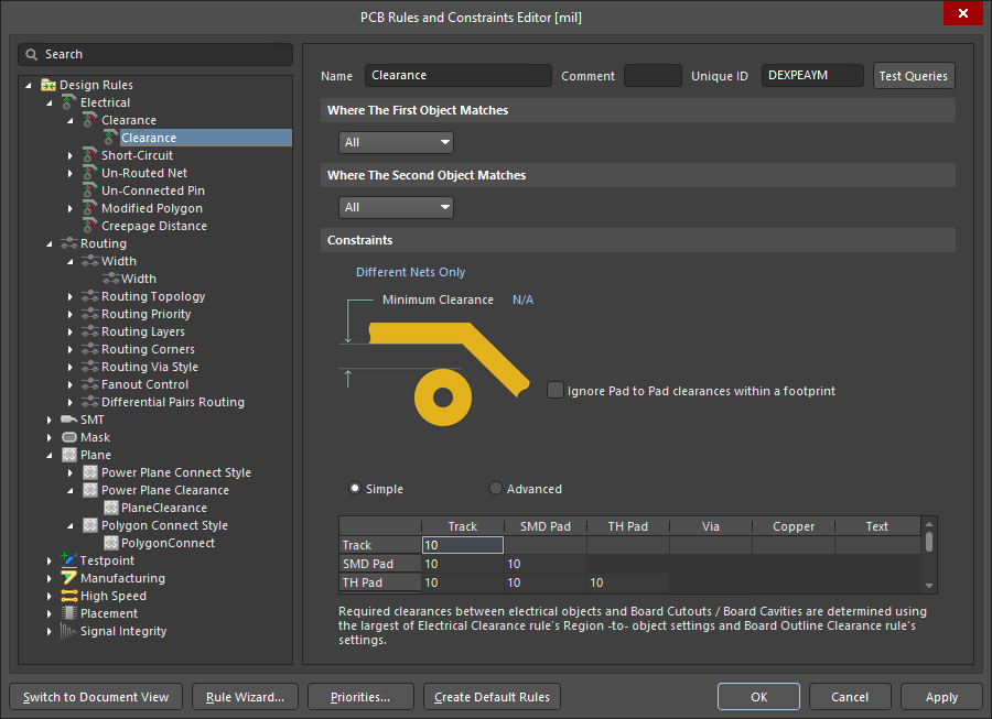
- Go to Design -> Rules… to view the PCB Rules and Constraints Editor
- Constraints set as such:
- Minimum clearance: 0.1524 mm (Electrical -> Clearance)
- Minimum trace width: 0.1524 mm (Routing -> Width)
- Minimum via diameter: 0.6 mm (Routing -> Routing Via Style)
- Copper to hole clearance: 0.3 mm (Electrical -> Clearance)
- Copper to Edge clearance: 0.4 mm (Manufacturing -> Board Outline Clearance)
- Minimum through-hole: 0.3 mm (Manufacturing -> Hole Size)
- Hole to hole clearance: 0.25 mm (Manufacturing -> Hole to Hold Clearance)
- Go to Design -> Layer Stack Manager… to set the number of electrical layers to two.
USB lines are routed as differential pairs
Given that USB lines are marked properly in the schematic as a differential pair, you can use interactive differential pair routing to ensure that they are routed to meet their required impedance and delay constraints.
On KiCad:
There’s this guide that’s really helpful for routing USB! The substrate parameters they assume are pretty close to what we’re using. We have absolutely no clue how controlled $\epsilon_{R}$ or ${tan(\delta)}$ is on the 2 layer boards that JLCPCB and PCBWay uses so ¯\(ツ)/¯ roll with the numbers on the site and you’ll probably be okay. If this makes you feel better, our demo boards have USB traces of 8 mils instead of the 30 mils recommended, and it works fine. I (Winnie) have also routed many many many boards without knowing what impedance matching is in the past, and all my stuff has worked so far. USB 2.0 is much more forgiving than what articles make it seem like. That being said, it can’t hurt to follow best practices.
- Go to File -> Board Setup -> Project -> Net Classes
- Select the Net Class belonging to the USB differential pairs or create a new one and assign them to it.
- Here, you can setup the clearance and width constraints for the differential pair (and its Net Class).
- Use Route -> Route Differential Pair to have KiCad automatically help you route the differential pair
- Click on one of the differential pair nets to begin routing.
On Altium:
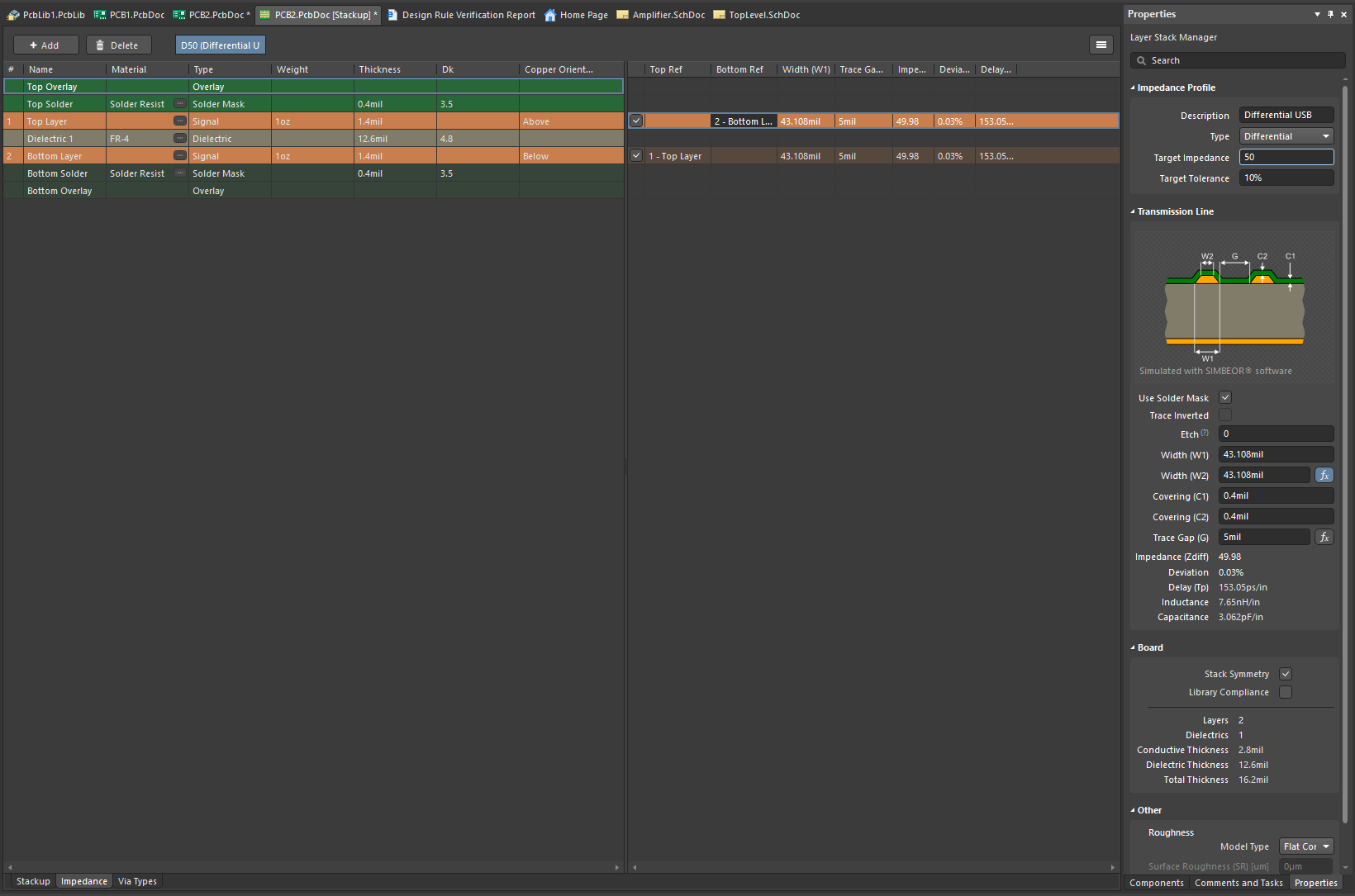
- To set up automatic differential impedance calculations, go to Design -> Layer Stack Manager… -> Impedance
- Here, you can create an impedance profile for differential signal route.
- Here, you can create an impedance profile for differential signal route.
- Regardless of if automatic impedance calculations are setup, differential routing rules can be enforced by going to Design -> Rules… -> Differential Pairs Routing
- Here, you can input parameters for how differential pairs should be routed and can even have the rule use the impedance profile set in the Layer Stack Manager
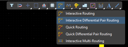
- Use the Interactive Differential Pair Routing tool on the USB data lines
- Altium will automatically route both differential pairs when you click on a net that is defined as being a differential pair
- Altium will automatically route both differential pairs when you click on a net that is defined as being a differential pair
PCB passes DRC (Design Rules Check)
KiCad: in the top, click on DRC and run it. You should see 0 errors and a relatively low number of warnings (<10). If you have lots of errors, fix your files or fix your layout. If there’s unrouted nets, route them.
DRC tool location (KiCad)
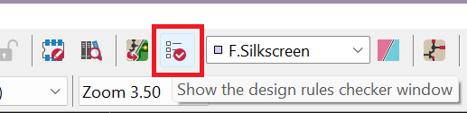
Altium: Go to Tools -> Design Rules Check… -> Run Design Rules Check. This will automatically generate a report with the errors found in your design, which are also listed in the messages panel. Clicking on the error messages will bring you to the location of the error in the PCB document.
Labeling
- Headers and testpoints are labeled with function, and if space permits, pinout
- Name, Board revision, board name exists on PCB in silkscreen
- Ensure markings that indicate the mounting or polarity of components for assembly are clearly visible and add additional markings as necessary
Labels generated using KiBlizzard, a KiCad Plugin
3D View
These allow for quick visual checks of the board particular for mechanical violations. However, doing so relies on footprints and their associated 3D models being accurate and placed/oriented correctly. It is a good practice use the 3D viewer as you layout your board as a quick check.
On KiCad, View -> 3D Viewer (Alt + 3).
On Altium, View -> 3D Layout Mode (number 3 key).
- Ensure footprint and silkscreen match the part model
- Part models do not collide
- Connectors face outwards and can be plugged in
- Soldermask is present where it should be and not present where it should not
Trace routing
- Traces do not make excessive turns and are as short as possible
- Vias used sparingly
- Trace width is appropriate for application
- Differential pairs (USB) routed as differential pairs
Adding MechE and Edgerton Logos
We want to thank MIT MechE and MIT Edgerton Center for sponsoring our class! Without them, none of this would be possible. To show our appreciation, we’d like you to include both logos in your PCB design. You can find their logos as footprints here for KiCad. They can be anywhere on your board, but we recommend a blank spot for the best look. Keep in mind they have no solder mask, so traces that aren’t the logo will get exposed.
Resources
- Winnie is an LA for 2.679 and has a FAQ for PCB design